

Shenzhen ICSLOVE Technology · PCB ADEPT

High-Quality Smd Pcb Assembly Manufacturer & Factory

Pioneering ultra-precision Surface Mount Device (SMD) and Surface Mount Technology (SMT) fabrication. Delivering zero-defect turnkey solutions, high-speed 01005 micro-component placement, fine-pitch BGA integration, and intelligent supply-chain resilience from Shenzhen's world-class electronic corridor.

Precision Engineering Solutions

High-Performance SMD & Advanced PCB Systems

Explore our certified array of high-frequency, flexible, rigid-flex, and embedded SMD architectures precision-tailored for radar, telecommunications, edge computers, and IoT terminals.


ODM High-Quality RF Microwave PCBs for Mobile Phones and Radar Systems
RF & Microwave

ODM High-Quality RF & Microwave PCBs for Mobile Phones and Radar Systems

OEM China Flexible PCB Suppliers Bending Folding Connections
Flex Technology

OEM China Flexible PCB Suppliers - Bending, Folding, Lightweight Connections

China High-Density Interconnect PCBs HDI Circuit Boards
HDI Class 3

China High-Density Interconnect PCBs | Quality HDI Micro-Via Circuit Boards

High Frequency PCB Suppliers Low Loss Signal Integrity
Low-Loss PTFE

High-Quality High Frequency PCB Suppliers: Signal Loss & EMI Solutions

Suppliers for RF Microwave PCBs 500MHz Frequency
Impedance Tuned

RF & Microwave PCBs - Low Loss, Controlled Impedance for ≥500MHz Frequency

High-Quality Raspberry Pi HAT Expansion Board SMT
Embedded Linux

High-Quality Raspberry Pi HAT Mini Single-Board Computer Expansion

Buy High Frequency PCBs Crosstalk and EMI Shielded
Ultra HF SMT

High Frequency PCBs - Minimize Signal Loss, Crosstalk, EMI & Impedance Mismatches

OEM China Raspberry Pi HAT Mini Computer SMT
IoT Integration

OEM China Raspberry Pi HAT: Single Board Mini-Computer Hardware Add-on

Industry Whitepaper Analysis

The Global SMD Assembly Imperative: Precision, Density, & Turnkey Execution

In modern electronics manufacturing, the transition from conventional plated through-hole (THT) circuitry to ultra-miniaturized Surface Mount Devices (SMD) constitutes the cornerstone of next-generation hardware innovation. As computing densities expand exponentially and operating frequencies transcend 500 MHz and multi-gigahertz thresholds, standard printed circuit board assemblies demand microscopic precision, impeccable solder joint integrity, and zero-defect thermal reflow management.

01005 & Ultra-Micro Placement

Mounting passive discrete chips down to 01005 (0.4mm × 0.2mm) and fine-pitch Ball Grid Arrays (BGA) with ball pitches below 0.35mm requires closed-loop optical alignment systems, advanced pick-up nozzle dynamics, and high-speed vibration-dampened feeder mechanisms.

  • YAMAHA Dual-Beam High Speed Mounters
  • Component range: 01005 up to 45mm² BGA
  • Dual-camera fiducial verification on-the-fly

Closed-Loop Solder Deposition

More than 65% of SMT production anomalies originate during solder paste printing. Implementing high-precision electropolished laser-cut stencils paired with 3D Solder Paste Inspection (SPI) guarantees absolute volumetric deposit compliance before component placement.

  • Real-time volume, height & area tracking
  • Automated stencil wipe & paste replenishment
  • Nano-coated electroformed stencils

Thermal Profiling & Intermetallics

Lead-free SAC305 (Sn96.5Ag3.0Cu0.5) alloys demand tightly managed nitrogen-inerted multi-zone reflow convection. Profiling guarantees optimal intermetallic compound (IMC) thickness of 1 to 3 microns, preventing brittle joint fracturing during mechanical stress.

  • Multi-zone convection with liquidus dwell control
  • Peak reflow Delta-T restricted to <2.5°C
  • Void minimization under BGAs/QFNs <15%
State-of-the-Art EMS Infrastructure

Inside Our 8,000 m² Shenzhen Manufacturing Facility

Founded in 2020 by Shenzhen ICSLOVE Technology Co., Ltd. in Anda Electronic Industrial Zone, Fuhai Subdistrict, Bao'an District, our facility synthesizes 15+ years of seasoned engineering mastery with 6 high-speed SMT lines and 4 specialized DIP wave-soldering cells.
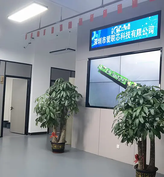
Shenzhen SMT PCB Assembly Clean Workshop Production Line

MES-Governed End-to-End Traceability

Every bare PCB entering our SMT line is laser-engraved with an internal serialized 2D DataMatrix code. Our custom Manufacturing Execution System (MES) maps every component reel, feeder slot, reflow thermal log, and optical inspection record directly to that unique board identity. In the event of a field anomaly, our Tier-1 and automotive customers can drill down to the specific component lot number, date code, operator shift, and reel supplier within 60 seconds.

99.8%
Quality Pass Rate
01005
Micro Package Spec
6 Lines
High-Speed SMT
3–9 Days
Fast Turn Prototypes
97%+
On-Time Delivery
500+
Global Accounts
Supply Chain Strategy

China Factory Supply Chain Resilience & Efficiency Advantage

Shenzhen's Bao'an District is globally acknowledged as the epicenter of hardware manufacturing agility. Known as China's Silicon Valley, the region fosters an unbroken supply ecosystem encompassing silicon wafer distribution, passive components fabrication, precision CNC enclosures, injection molders, and express international air freight hubs.

The 2-Hour Sourcing Perimeter

Within a two-hour transit perimeter from our Bao'an facility, our procurement department interfaces directly with factory-authorized distribution centers representing Texas Instruments (TI), Analog Devices (ADI), STMicroelectronics, Microchip, Murata, TDK, and TE Connectivity (Tyco). Urgent prototype iterations obtain authentic components on the same calendar day.

Drop-In BOM Optimization (Cost-Down)

Global semiconductor allocations and obsolescence cycles frequently disrupt western production schedules. Our seasoned component engineering team conducts exhaustive BOM scrubbing, identifying form-fit-function (FFF) pin-to-pin drop-in alternatives that consistently compress raw bill-of-materials expenditures by 10% to 25% without sacrificing reliability.

Counterfeit Prevention & IQC Verification

Our Incoming Quality Control (IQC) protocol integrates deep decapsulation testing, X-ray lead-frame inspection, solderability testing, and microscopic markings analysis. Every component batch is matched against manufacturer datasheets, guaranteeing that counterfeit, aged, or compromised semiconductor inventory never reaches the feeder cart.

Diverse Mission Profiles

Localized Applications & Field-Proven Vertical Environments

SMD PCB assemblies manufactured by PCB ADEPT are engineered to endure rigorous field stressors across distinct geographic and commercial microclimates—from sub-zero Arctic radar outposts to high-vibration automotive chassis.

RF, Microwave & Drone Jamming

Critical RF systems require ultra-low dielectric dissipation factors (Df < 0.002) and controlled coplanar waveguide layouts. Utilizing Rogers 4350B, RO4003C, and Taconic hybrid PTFE multi-layer stack-ups, our SMT lines populate power amplifiers, RF switches, and high-frequency stripline filters with continuous 50-ohm characteristic impedance matching.

  • Operating bandwidth: 500 MHz up to 40 GHz
  • Applications: Anti-drone systems, 5G base stations, military radar

Automotive Power & EV BMS

Automotive electronics mandate zero thermal degradation under high mechanical shocks. We assemble heavy copper (up to 4oz) SMD boards incorporating high-thermal conductivity aluminum backplanes, mounting MOSFETs, shunt resistors, and microcontrollers for Electric Vehicle (EV) Battery Management Systems (BMS) and on-board DC-DC converters.

  • Thermal cycle endurance: -40°C to +125°C
  • Applications: Inverters, charging piles, automotive telematics

Medical Diagnostic & Wearables

Miniaturized health trackers and diagnostic probes require dense High-Density Interconnect (HDI) rigid-flex circuit boards with microscopic micro-vias and 01005 passives. Assembled within ESD-controlled, cleanroom-standard cells, these PCBA assemblies guarantee uninterrupted biological signal acquisition and bio-compatibility.

  • Class 3 IPC-A-610 medical-grade soldering
  • Applications: Wearable ECG monitors, blood analyzers, endoscopy probes

Industrial Automation & Edge AI

Factory automation environments present aggressive dust, moisture, and chemical vapor challenges. Our turnkey service coats assemblies with automated silicone, polyurethane, or acrylic conformal coatings, protecting high-pin-count microprocessors, optical isolators, and relay controllers against harsh industrial corrosion.

  • Automated selective spray conformal coating
  • Applications: PLC controllers, machine vision modules, smart robotics

Aerospace & Satellite Telemetry

Outgassing constraints and cosmic radiation resistance necessitate premium substrate finishes such as Electroless Nickel Electroless Palladium Immersion Gold (ENEPIG) and thick hard gold plating. Combined with high-Tg FR-4 (>180°C) and polyimide flex layers, our assemblies maintain physical structural integrity during extreme thermal shock.

  • ENEPIG & Hard Gold wire-bondable surfaces
  • Applications: CubeSat bus avionics, high-altitude UAV payloads

IoT Nodes & Single-Board Computers

For smart cities and distributed sensing grids, we engineer cost-optimized Raspberry Pi HAT modules and ultra-low-power LoRa/NB-IoT sensor boards. Leveraging high-volume automated SMT pick-and-place lines, we enable agile transition from rapid prototyping batches (1–500 pcs) directly into mass runs exceeding 100,000 units.

  • Multi-sensor integration on 4–6 layer rigid-flex
  • Applications: Smart agriculture, utility metering, asset trackers
Technical Verification Matrix

Engineering Specifications & SMT Manufacturing Boundaries

A rigorous engineering reference matrix illustrating our baseline tolerances, component compatibility, and quality verification standards across all 6 SMT lines.

Process / Metric Factory Capability & Parameter Quality Assurance Method
Smallest SMT Package 01005 (0.4mm × 0.2mm) & 0201 passives Dual-CCD high resolution camera alignment
Fine-Pitch BGA Placement Ball pitch down to 0.30mm; micro-BGA, QFN, CSP, PoP 3D X-Ray inspection (AXI) < 15% voiding
Rigid PCB Layers Standard: 1–8 layers | Advanced Builds: Up to 32 layers Flying probe & bed-of-nails electrical test
Flex & Rigid-Flex PCBs Flex: 1–6 layers | Rigid-Flex: 4–22 layers (up to 4x HDI) Cross-section microsectioning & peel testing
Base Substrates FR-4 (Tg 130–180°C), Rogers, Taconic, Polyimide, Aluminum Core Incoming Material Certificate of Analysis (CoA)
Surface Finishes ENIG, ENEPIG, Immersion Silver, Immersion Tin, Hard Gold, OSP X-Ray Fluorescence (XRF) coating thickness test
Solder Paste Deposition Full-automatic electro-polished laser stencil with nano-coating 3D SPI (Solder Paste Inspection) 100% volume
Inspection Spectrum IQC → 3D SPI → Pre-Reflow AOI → 3D Post-Reflow AOI → AXI → FCT Real-time MES SPC drift alarms & logging
Compliance & Workmanship IPC-A-610 Class 2 & Class 3 | ISO 9001:2015 | UL 94V-0 | RoHS | REACH Certified IPC-A-610 trainers on assembly floor
Future Innovations

SMT Roadmap: 2026–2030 Advanced Assembly Horizon

As microelectronics miniaturization asymptotically approaches physical lithographic limits, surface-mount engineering is transitioning toward heterogeneous 3D integration, active substrate embedding, and artificial-intelligence-governed self-correcting fabrication lines.

Sub-01005 (008004) SMT Scaling

Next-generation ultra-dense wearables and silicon-in-package (SiP) architectures mandate component placement for 008004 passives measuring merely 0.25mm × 0.125mm. Our advanced line testing integrates ultra-precision vacuum-feedback pick tips, high-acceleration linear motors, and anti-static ion-controlled placement chambers.

Embedded Component Packaging (ECP)

To eliminate surface routing congestion and suppress parasitic inductance in high-speed 6G RF links, we are actively expanding substrate cavity embedding technologies. Passive inductors, bypass capacitors, and ultra-thin bare dies are vacuum-laminated directly inside internal inner dielectric cores, freeing 100% of the surface layer for dense ICs.

AI Predictive Closed-Loop Synthesis

By connecting 3D SPI and post-reflow 3D AOI inspection stations via an edge AI neural controller, our automated printers actively compensate squeegee blade pressure, print speed, and separation angles dynamically before any solder bridge, insufficient wetting, or tombstoning defect can materialize.

Regulatory & Engineering Assurance

Localized Engineering Support & Global Compliance Framework

Collaborating with an overseas assembly partner requires uncompromised communications, swift DFM feedback, and strict adherence to international regulatory baselines. We provide English-speaking senior design engineers directly assigned to your account, bridging technical time zones effortlessly.

Comprehensive DFM / DFA / DFT Audits

Prior to cutting stencils or kitting materials, our engineering group subjects your Gerber (or ODB++) data, XY centroid files, and BOM to a multi-point Design for Manufacturability audit. We inspect trace-to-pad clearances, solder mask dam width, thermal relief balancing, and test-point accessibility to prevent solder bridges and tombstoning.

IPC-A-610 Class 2 & Class 3 Workmanship

Whether assembling standard consumer hardware under IPC Class 2 or high-reliability life-support, industrial, or aerospace equipment under IPC Class 3, our certified IPC quality inspectors verify barrel fill percentages (>75% on through-holes), heel fillet wetting, and solder coverage with calibrated optical and X-ray tools.

Full Turnkey Box Build & Logistics

Beyond board-level SMT assembly, PCB ADEPT delivers complete electro-mechanical box build integration. We handle custom CNC milling, plastic injection molding, wire-harness crimping, firmware flashing, functional testing (FCT), custom retail packaging, and door-to-door express customs delivery across North America, Europe, and Asia-Pacific.

Industrial & RF Catalog

Specialized Substrates, Rigid-Flex & Expansion Boards

Explore our specialized range of high-thermal aluminum substrates, multi-layer rigid-flex solutions, micro-via HDI boards, and OEM customized expansion HAT assemblies manufactured in Shenzhen.


OEM China Raspberry Pi HAT Expansion Board Solutions
SBC Expansion

OEM China Raspberry Pi HAT Suppliers - Enhance Your Hardware Projects

ODM High-Quality RF Microwave PCBs Radar Systems
High Frequency

ODM High-Quality RF & Microwave PCBs for Mobile Phones & Radar Systems

OEM China RF Microwave PCB Suppliers 500MHz+
Low Signal Loss

OEM China RF & Microwave PCB Suppliers - Low Loss, Impedance Controlled

High Thermal Conductivity Aluminum PCB Power Circuit
Metal Core SMT

China High Thermal Conductivity Aluminum PCB for High-Power Circuitry

ODM China Rigid Flex PCB 4 to 16 Layer Multi-Layer
Rigid-Flex Multi

ODM China Rigid Flex PCB Suppliers - 4–16 Layer Complex Multi-Layer

ODM High Density Interconnect HDI PCB Advanced Circuit
Micro-Via Laser

ODM High Density Interconnect (HDI) PCB for Advanced Mobile & Computing

Buy High-Density Interconnect HDI PCB Factory SMT
HDI Factory Direct

Buy High-Density Interconnect HDI PCB from Leading China Factory

ODM China Rigid Flex PCB Suppliers Quotes
4-16 Multi-Layer

ODM China Rigid Flex PCB: Single & Double-Sided 4–16 Layer Solutions

Procurement & Engineering FAQ

Frequently Asked Questions on SMD PCB Assembly

In-depth answers addressing design tolerances, procurement logistics, quality guarantees, and manufacturing parameters for global hardware development teams.

What is the minimum order quantity (MOQ) and lead time for SMD PCBA prototypes?
Our prototype SMD PCBA service starts from 1 piece up to pilot production runs of 500 pieces, enabling seamless R&D functional verification without tying up capital in excessive inventory. Standard prototype lead time ranges between 3 to 9 business days from the moment the bare PCBs are fabricated and BOM components are checked in through IQC. For expedited projects, rapid 48-to-72-hour SMT turnaround options are available depending on component complexity and stock availability.
What engineering files are strictly required to quote and begin SMD assembly?
To provide an exact quote and initiate automated SMT programming, we require:
  • Gerber RS-274X or ODB++ files: Encompassing all copper trace layers, solder mask, silkscreen, and board edge outline.
  • Complete Bill of Materials (BOM): Formatted in Excel or CSV, explicitly detailing Reference Designators (e.g., R1, C2, U3), exact Manufacturer Part Numbers (MPN), approved alternate brands, package footprints, and quantities per board.
  • Centroid / Pick-and-Place (XYRS) file: Specifying component reference, center coordinates (X and Y in mm or mils), board surface side (Top/Bottom), and component rotation angle (0° to 360°).
  • Assembly Drawings & Work Instructions: Clarifying polarized component directions, connector heights, masking areas, or manual soldering guidelines.
How does PCB ADEPT guarantee component authenticity and prevent counterfeit parts?
Our procurement division has operated in Shenzhen for over 15 years, maintaining direct relationships with authorized global semiconductor distributors (such as Mouser, DigiKey, Arrow, and Avnet) alongside direct factory tier-1 channel partners representing TI, STMicroelectronics, ADI, NXP, Microchip, and Murata. All incoming reels, trays, and tubes undergo mandatory Incoming Quality Control (IQC) containing barcoded traceability, packaging integrity verification, pin oxidation analysis, microscope marking authentication, and random X-ray leadframe inspection. We never purchase active semiconductors from untracked spot markets without formal customer authorization and internal lab clearance.
Can you assemble fine-pitch BGAs, QFNs, and micro 01005 chips on the same board?
Yes. Our 6 high-speed YAMAHA SMT production lines are calibrated to handle mixed-density boards combining ultra-miniature 01005 passives alongside complex Ball Grid Arrays (BGA) with pitches as narrow as 0.30mm, Quad Flat No-Lead (QFN) packages, and Chip Scale Packages (CSP). By combining high-precision laser-cut stencils, step-down stencil technology where necessary, and automated 3D Solder Paste Inspection (SPI), we achieve uniform solder paste volume across both microscopic pads and larger thermal ground slugs.
What quality inspection procedures are executed during the SMT production flow?
Quality assurance at PCB ADEPT is executed at multiple synchronous stages under our ISO 9001:2015 management system:
  1. IQC (Incoming Quality Control): Validates raw PCB dimensions, surface finish thickness, and BOM component authenticity.
  2. 3D SPI (Solder Paste Inspection): 100% inline measurement of paste deposit height, area, volume, and bridge offset before placement.
  3. Pre-Reflow AOI: Verifies component placement presence, polarization, and alignment prior to heating.
  4. Multi-Zone Reflow Convection: Nitrogen-inerted thermal profiling monitored with real-time Datapaq thermocouple profilers.
  5. 3D Post-Reflow AOI: Validates solder joint meniscus, wetting angles, tombstones, solder balls, and pin bridging.
  6. AXI (Automated X-Ray Inspection): Verifies hidden BGA ball sphericity, void percentages (< 15%), and QFN thermal pad wetting.
  7. FAI (First Article Inspection): Dedicated engineering verification of the initial board off the line against full schematics.
  8. FCT (Functional Circuit Testing): Custom test jigs, firmware programming, voltage rail verification, and full-load burn-in chambers.
Do you support RoHS, lead-free reflow, and UL certification requirements?
Yes, 100% of our standard production lines operate in strict adherence to RoHS 3 (Directive 2015/863/EU) and REACH (EC 1907/2006) regulations, utilizing lead-free SAC305 (Sn96.5/Ag3.0/Cu0.5) or low-temperature tin-bismuth solders. Furthermore, all raw PCB laminates used are UL certified with a 94V-0 flame retardancy rating. Complete Material Declarations, RoHS Declarations of Conformity, and Certificates of Compliance (CoC) are issued upon product shipment for global customs clearance.
What is the difference between Partial Turnkey and Full Turnkey PCBA?
In Full Turnkey Assembly, PCB ADEPT manages every link in the chain: manufacturing the raw printed circuit boards, sourcing 100% of the active and passive electronic components from certified distributors, fabricating the laser stencils, performing SMT and through-hole soldering, executing optical/X-ray testing, and packaging the finished product. In Partial Turnkey (Consignment), the customer supplies specific critical components (such as proprietary pre-programmed MCUs, custom ASICs, or specialized sensors), while our facility fabricates the bare PCBs and sources the remaining standard passives, connectors, and hardware.
How does PCB ADEPT protect intellectual property (IP) and confidential firmware?
We operate under strict, legally enforceable non-disclosure agreements (NDAs). Customer design files, schematics, and firmware binaries are stored in encrypted, isolated on-premise servers with restricted role-based engineering access. Firmware flashing programming fixtures are operated via locked workstations without external USB or unauthorized internet connectivity, ensuring complete data security from initial quote to final box build delivery.

