
Top 5 Qualities to Look for in a Reliable OEM Flexible PCB Board Manufacturer in 2026
How to vet flex PCB suppliers on materials, lamination control, inspection and supply chain resilience as device designs shrink.
Continue reading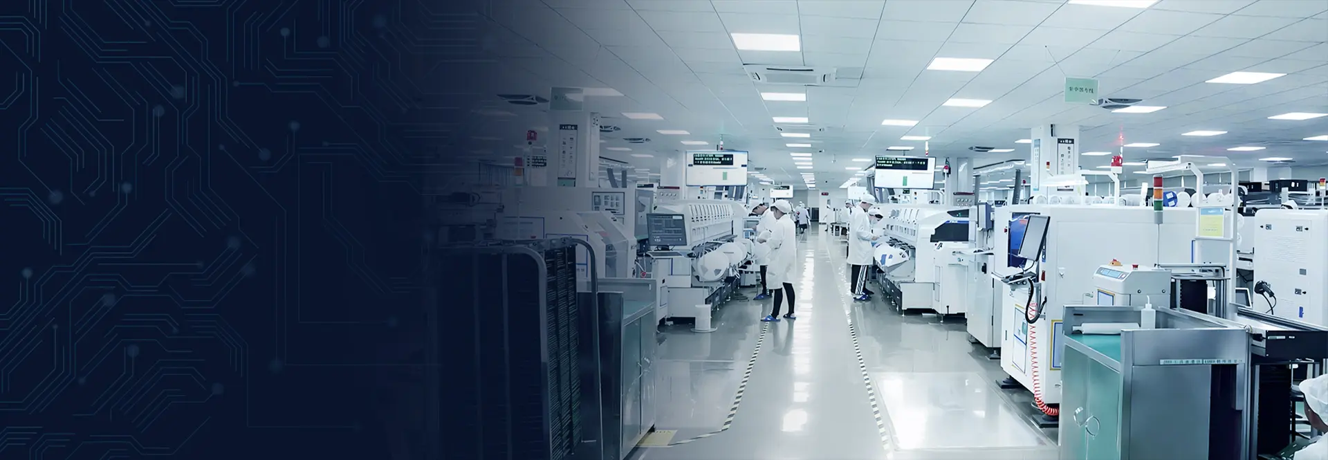

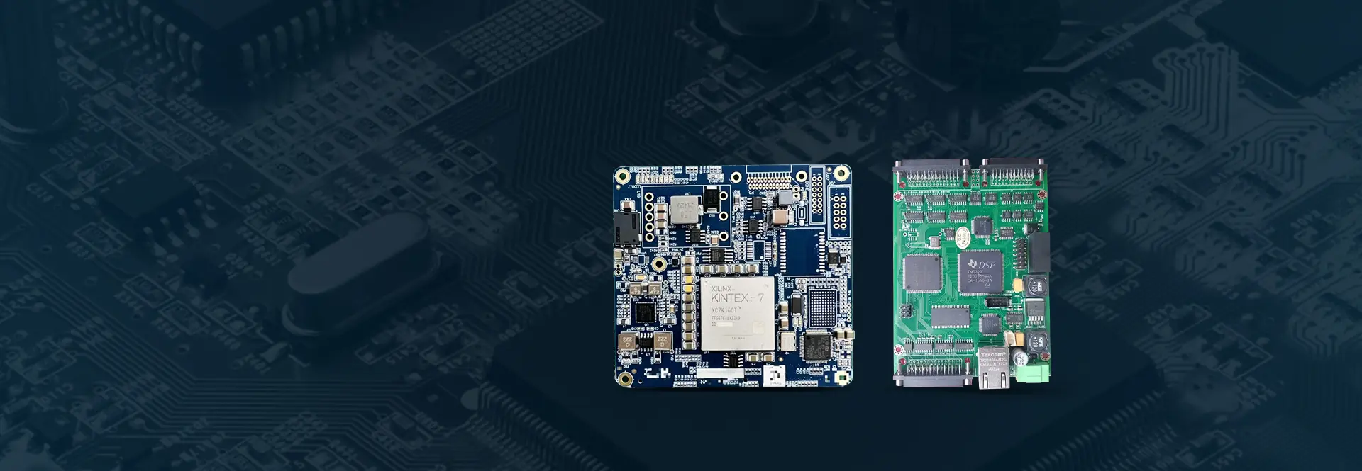
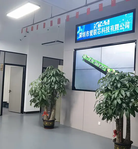
PCB ADEPT is the export brand of Shenzhen ICSLOVE Technology, an electronics manufacturing partner that takes your project from bare board and component sourcing to tested, packed finished products.
Founded in 2020 in Shenzhen — China's "Silicon Valley" and home to Huawei, BYD and DJI — our engineering and production team brings more than 15 years of hands-on PCB and EMS experience. We serve industrial control, automotive, telecom, medical, aerospace, IoT and anti-drone customers, supporting fast prototypes, pilot runs and full-scale production under one quality system.
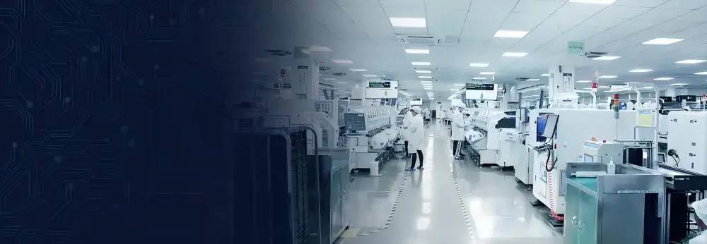
6 SMT lines, 4 DIP lines and an 8,000 m² workshop, tracked end-to-end by a Manufacturing Execution System (MES).
Build-to-print manufacturing, DFM feedback, reverse engineering and product replication for legacy or end-of-life boards.
Overseas buyers lose time and margin juggling separate board shops, assemblers and brokers. We consolidate the four critical stages under one contract, one project engineer and one traceable quality record.
BOM review, sourcing of TI, ADI, ST, Microchip, Murata and TE (Tyco) parts, alternates for long-lead items and shared stock of common components.
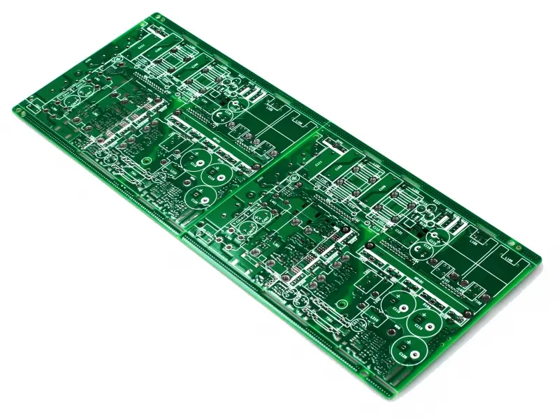
Rigid, flex, rigid-flex, HDI and RF/microwave boards built to your stack-up, material and surface finish requirements.
SMT and through-hole assembly with SPI, AOI and 3D AOI inspection, with every lot recorded in MES for full traceability.
Enclosure integration, firmware programming, functional testing, aging, labeling, packing and worldwide shipment.
Key process parameters are listed on every card so your engineering team can pre-qualify fit before the first call.
 PCB
PCB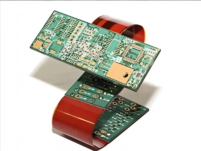 PCB
PCB PCB
PCB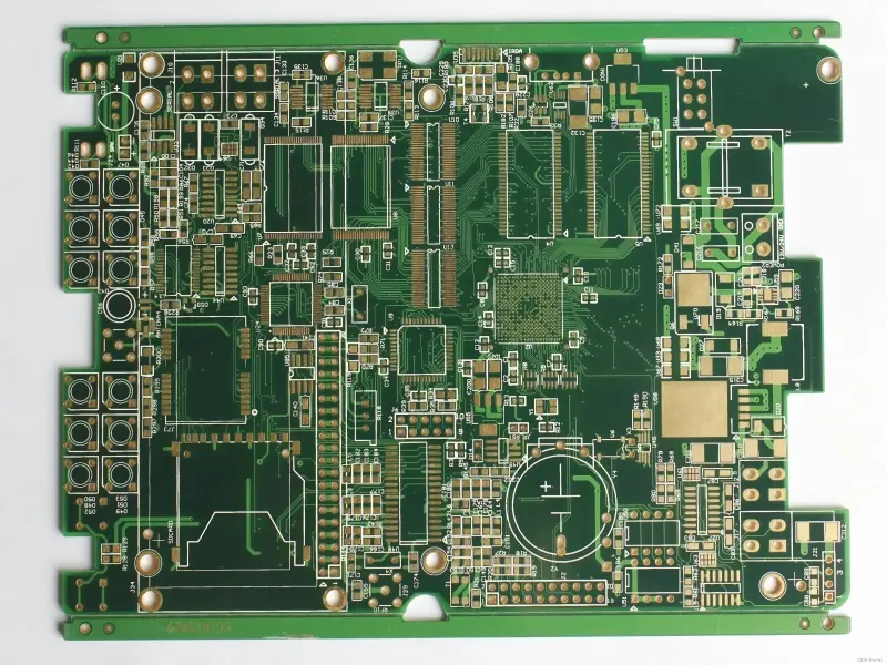 PCB
PCB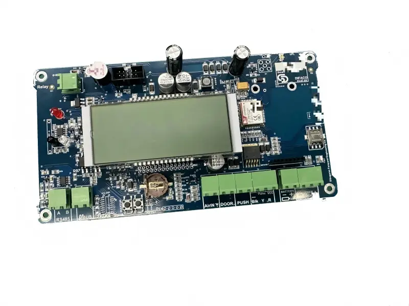 Fast-Turn
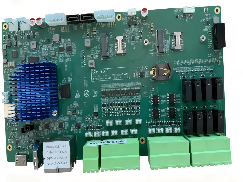 PCBA
PCBA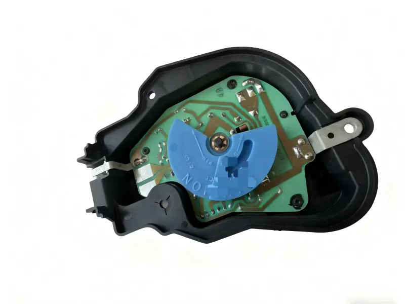 Box Build
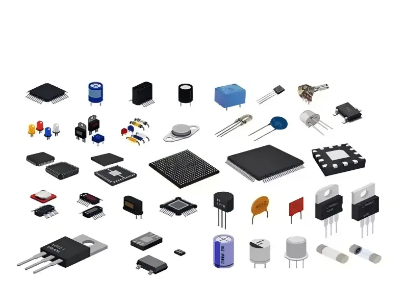 Sourcing
Compare our PCB, PCBA and sourcing programs, or get the full capability catalog with stack-up options, tolerances and inspection standards.
Select a station to see where it sits in the build flow and what it controls. Every stage below feeds data into our MES so each board can be traced back to its materials, operators and inspection results.
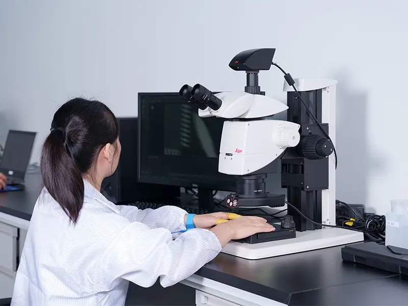
Components and bare boards are checked against the BOM and datasheets before kitting, so counterfeit, mislabeled or damaged parts never reach the line.
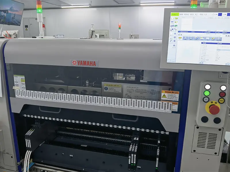
High-speed YAMAHA mounters handle everything from micro passives to fine-pitch BGAs, keeping prototypes and volume runs on the same proven platform.
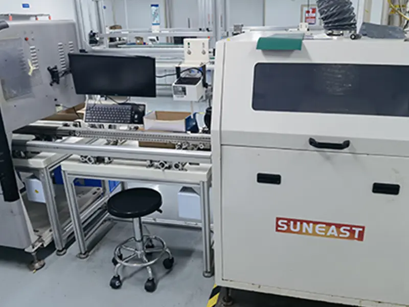
Pre-reflow optical inspection catches missing, shifted or wrong-polarity parts while they can still be corrected without rework, protecting first-pass yield.
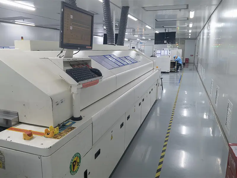
Thermal profiles are set per product according to board mass and component mix, giving consistent solder joints on mixed BGA and fine-pitch assemblies.
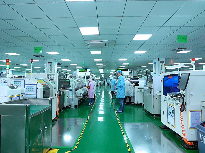
A controlled SMT floor runs parallel lines so urgent prototypes do not wait behind production orders, and volume lots can be split across lines.
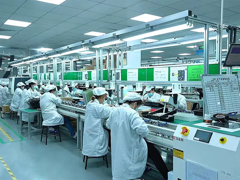
Each line integrates solder paste printing, SPI, placement, reflow and AOI, so inspection data is captured at every step of the build.
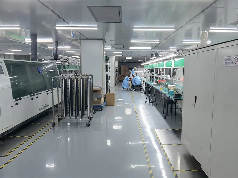
Dedicated through-hole lines cover connectors, transformers and power components, with wave and selective hand soldering for mixed-technology boards.
Planning a supplier audit? Get our equipment list and quality documentation in the capability catalog.
Get the Factory CatalogA quick DFM checklist for procurement and hardware engineers comparing Shenzhen PCB assembly suppliers.
| Capability | Specification |
|---|---|
| Rigid PCB layers | 1–8 layers standard; higher layer counts on advanced builds |
| Flex / Rigid-flex | Flex 1–6 layers; rigid-flex 4–22 layers; HDI lamination cycles up to 4x |
| Base materials | FR-4, CEM-1, aluminum, copper base, Rogers, Taconic, hybrid stacks |
| Surface finishes | Hard gold, ENIG, ENEPIG and standard finishes |
| Assembly technology | SMT and THT; lead-free (RoHS) reflow and wave soldering |
| Component range | 01005, 0201, 0402, 0603, 0805, fine-pitch ICs and BGA |
| Inspection & test | IQC, SPI, AOI, 3D AOI, FAI, functional test (FCT), aging |
| Prototype volume & lead time | 1–500 pcs; 3–9 days typical |
| Quality & compliance | ISO 9001 quality system; UL and RoHS compliant production; MES traceability |
Final capability depends on design complexity and material availability. Our engineers confirm feasibility during DFM review before production starts.
Measured performance, not marketing claims — the numbers our customers in 50+ countries hold us to.
Core team expertise in PCB fabrication and electronics manufacturing.
From start-ups to established OEMs across 50+ countries.
Verified through SPI, AOI, FAI and functional testing.
MES-based scheduling keeps prototypes and production on plan.
Long-term repeat business from domestic and overseas clients.
Through BOM optimization and alternatives, with free sample support.










Each sector brings different reliability, compliance and material requirements. Our process windows are tuned accordingly.

Low-loss Rogers and Taconic boards and hybrid stacks for antennas, modules and base-station electronics.

RF power, detection and jamming electronics where signal integrity and thermal control are critical.

Radar and satellite boards with hard gold or ENEPIG finishes and full lot traceability.

Cost-optimized, high-volume assemblies with BOM alternatives that protect margins.

Copper and aluminum base PCBs plus THT power components for inverters, chargers and BMS.

Long-lifecycle controller boards with reverse engineering support for legacy designs.

Compact wireless modules with 0201/01005 passives, MCU programming and box build.

Prototype circuit boards for wearable health trackers and diagnostic devices with documented inspection.
Send your Gerber and BOM and receive engineering feedback from people who build boards every day — not a sales script.
Practical guidance for engineers and buyers evaluating PCB and PCB assembly suppliers.
How to vet flex PCB suppliers on materials, lamination control, inspection and supply chain resilience as device designs shrink.
Continue reading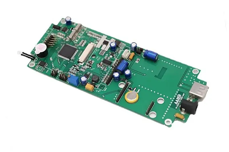
PCBA (printed circuit board assembly) covers the entire process of mounting and soldering components onto a bare board, from paste printing to testing.
Continue reading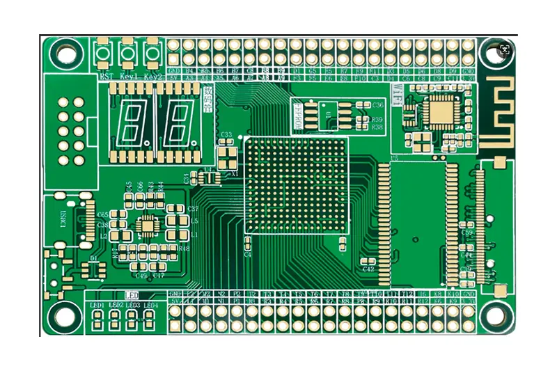
A PCB (printed circuit board) is the foundational building block of almost every electronic device, connecting components through copper traces.
Continue reading
Since May 2025, Shenzhen ICSLOVE Technology Co., Ltd. has operated from its new facility in Anda Electronic Industrial Zone, Fuhai, Bao'an District.
Continue readingStraight answers to the questions procurement teams ask most before placing a first order with a Chinese PCBA manufacturer.
Prototype and trial-run PCB assembly starts from 1 piece and covers quantities up to around 500 pcs, with a typical lead time of 3–9 days depending on board complexity and component availability.
Send Gerber files (or ODB++), a complete BOM with manufacturer part numbers, a pick-and-place (centroid) file and assembly drawings. Test instructions or firmware are needed if you require programming or functional testing.
Quality is controlled at every stage: IQC for incoming materials, SPI for solder paste, AOI before and after reflow, 3D AOI, first article inspection (FAI) and functional testing (FCT), all recorded in a Manufacturing Execution System (MES) under an ISO 9001 quality system.
Yes. The sourcing team has over 10 years of experience procuring parts from brands such as TI, ADI, ST, Microchip, Murata and TE Connectivity (Tyco), and keeps an inventory of common components. Alternative parts are proposed when lead time or cost is a risk.
Manufacturing operates under an ISO 9001 quality management system, and PCBs and assemblies can be produced to UL and RoHS (lead-free) requirements.
Yes. Beyond PCBA, the factory supports plastic enclosure molding, CNC machining, 3D printing, memory and MCU programming, finished product testing, aging, labeling, packaging and international delivery.