
Buy High-Density Interconnect HDI PCB from China - Quality Products by Leading Suppliers and Factory Manufacturers, Factories
Product Description
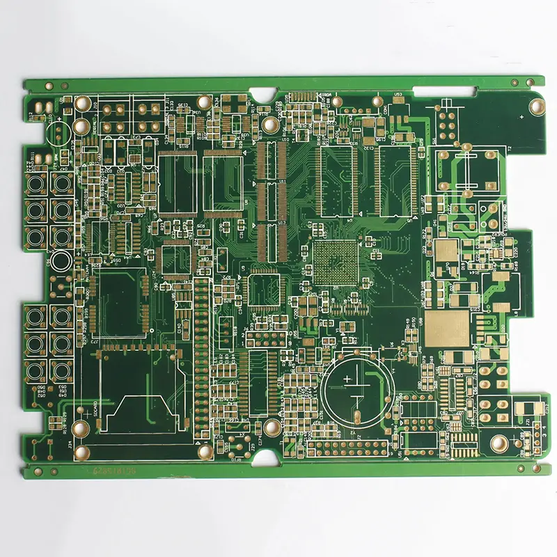
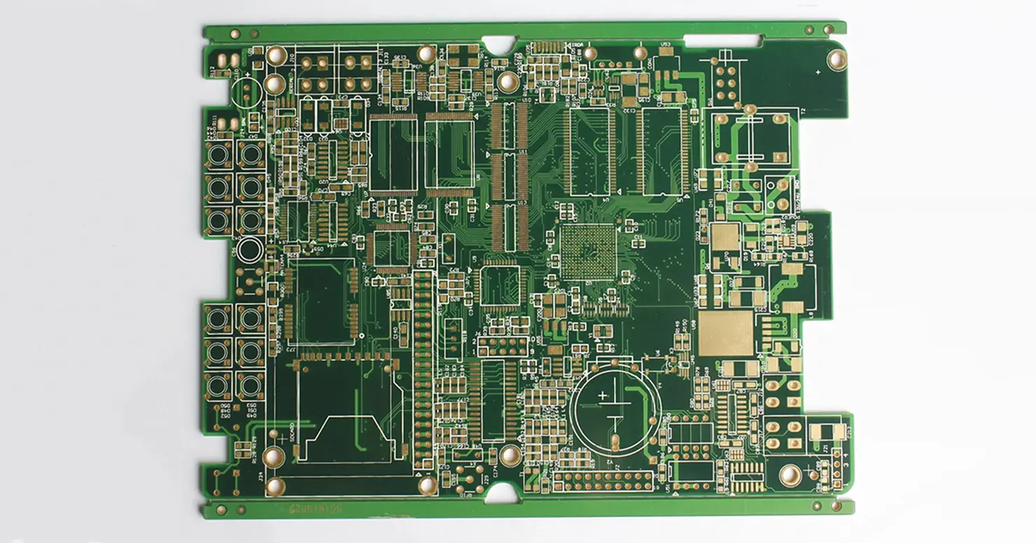
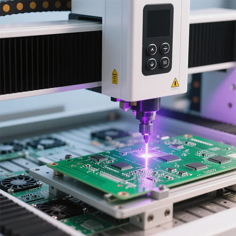
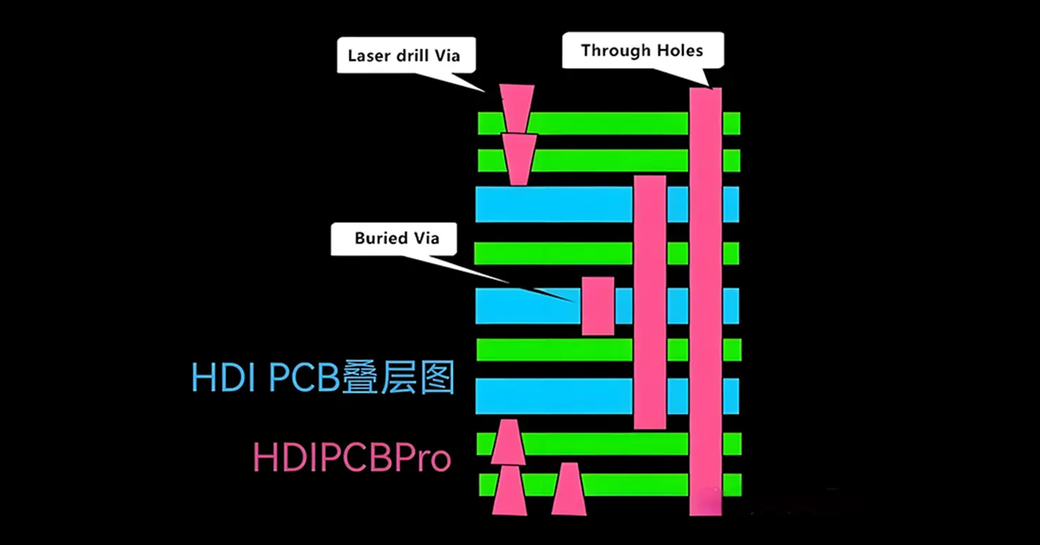
HDI PCB (High Density Interconnect PCB) refers to a high-density interconnect printed circuit board. Its core feature is realizing interconnection between different copper layers through laser-drilled micro blind vias and buried vias. Compared with traditional PCBs, it can integrate more circuits and components in a smaller area, and is often used in miniaturized high-end electronic products such as smartphones and wearable devices.
HDI PCBs are classified into low-order types (e.g., 1st-order, 2nd-order) and high-order types (3rd-order and above) based on the number of build-up layers. High-order products usually adopt any-layer interconnection technology. By shortening signal paths through microvias, it optimizes signal integrity and adapts to high-frequency and high-speed data transmission scenarios.
| Design Considerations | Specifications & Explanations |
| Control of Line Width and Spacing | For mainstream processes, the minimum line width and spacing are recommended to be no less than 4mil (approximately 0.1mm). Although high-end processes can support 3mil or even 2.5mil, a margin of more than 20% should be reserved to prevent wire breakage, short circuits, and other issues during etching. |
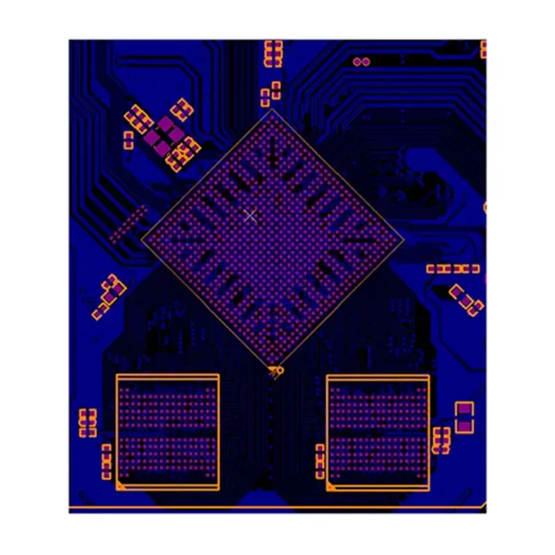
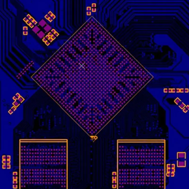
| Via Structure Design | Prioritize controlling laser blind vias to 1–2 orders with a via size of no less than 0.15mm; when using via-in-pad for BGA packages, proper hole plugging design is required; use stepped blind vias as much as possible and reduce stacked blind vias to lower the risk of alignment deviation. |
| Optimization of Stackup Planning | Divide the functions of each layer according to signal types in advance. For example, adopt an alternating layout of signal layers, ground layers, and power layers (e.g., 1st layer: signal layer, 2nd layer: ground layer, 3rd layer: power layer) to improve electromagnetic compatibility (EMC) and signal stability. |
| Pad and Thermal Design | The pad diameter is recommended to be larger than 0.3mm, with a reasonable spacing from vias; select thermally conductive materials such as ceramic substrates, add copper blocks or thermal vias under heat-generating components, and increase copper foil reinforcement layers to expand the heat dissipation area. |
| Manufacturability Consideration | Comply with design standards such as IPC-2226 and reserve 10%–20% manufacturing tolerance for parameters. For example, the offset between the pad center and via center should not exceed 0.075mm to avoid rework caused by parameters being too close to process limits. |
| Production Considerations | Specifications & Explanations |
| Material Compatibility Control | When selecting substrates, prepregs, and other materials, match their coefficients of thermal expansion (CTE) to avoid warpage and delamination after lamination; verify material compatibility through pre-tests if necessary, and choose solder mask inks with strong adhesion and good temperature resistance. |
| Lamination Precision Control | Adopt high-precision alignment systems to control interlayer offset errors during multilayer board lamination; prioritize symmetrical even-layer stacking and maintain stable lamination parameters within an appropriate range to prevent defects such as bubbles and insufficient resin filling. |
| Microvia Processing Quality | Use laser drilling machines to ensure the aperture precision of 0.1mm–0.15mm microvias, and promptly remove residual impurities on hole walls after drilling; during subsequent electroless copper plating and electrolytic copper plating, ensure uniform plating on hole walls to avoid voids and fractures. |
| Cleanliness and Environmental Control | Maintain a high level of cleanliness in the production environment; thoroughly remove contaminants after processes such as etching and cleaning to prevent plating peeling and circuit failures of microvias and fine circuits due to pollution. |
| Enhanced Inspection Processes | Use AOI (Automated Optical Inspection) equipment to detect surface defects of circuits; use X-ray to inspect the alignment of blind vias/buried vias and BGA solder joint quality; verify electrical performance through flying probe tests and ICT (In-Circuit Test) to ensure impedance deviation is within a reasonable range. |
| Equipment and Process Calibration | Regularly calibrate equipment such as CNC drilling machines and laminators, and real-time monitor key parameters such as lamination temperature and electroplating current; establish standardized operating procedures for processes such as etching and development to reduce process fluctuations. |
PCB (Printed Circuit Board), also known as printed wiring board in Chinese, is an important electronic component. It serves as the support for electronic components and the carrier for their electrical connections. Because it is made by electronic printing technology, it is called a "printed" circuit board.
Its main function is that after electronic devices adopt printed circuit boards, due to the consistency of similar printed circuit boards, errors in manual wiring are avoided. It can also achieve automatic insertion or surface mounting of electronic components, automatic soldering, and automatic detection, ensuring the quality of electronic devices, improving labor productivity, reducing costs, and facilitating maintenance.
HDI boards are high-density interconnect circuit boards. Boards with blind hole electroplating and secondary lamination are all HDI boards, which are classified into first-order, second-order, third-order, fourth-order, fifth-order, etc. For example, the mainboard of iPhone 6 is a fifth-order HDI.
| HDI CAPABILITY | |||||
| HDI PCB | HDI PCB Steps range | 1-3 Steps HDI | 1-6 Steps HDI | ||
| Laser hole range | 4-6 MIL | 3-6 MIL | |||
| Aspect Ratio of Laser Blind Via | 1 Step | 0.5∶1 ~ 0.8∶1 | ≤0.9∶1 | ||
| 2 Steps or more | 0.5∶1 ~ 0.8∶1 | 0.5∶1 ~ 0.8∶1 | |||
| Dielectric Thickness of Laser Blind Via | 2.5~4 MIL | 2.5~5 MIL | |||
| Bottom Pad Annular Ring (mil) | D+8MIL (D = Laser Via Diameter) | D+6MIL (D = Laser Via Diameter) | |||
| Laser Blind Via Pad Annular Ring | 1 Step | 4 MIL | 4 MIL | ||
| 2 Steps or more | 5 MIL | 4 MIL | |||
| Micro Via Fill Protrusion/Depression (Max.) | Maximum protrusion 50μm, maximum depression 127μm | ||||
| Max. Panel Size | Thickness < 0.6MM | Panel size ≤ 415×520MM (shipping size: 375×480MM) | |||
| Thickness ≥ 0.6MM | Panel size ≤ 470×620MM (shipping size: 430×580MM) | ||||
-
Q1 What are the typical via sizes in HDI PCBs?HDI PCBs typically use microvias with diameters ranging from 50–150μm (2–6 mils), significantly smaller than traditional PCB vias of 250–300μm.
-
Q2 How much smaller can HDI PCBs be compared to traditional PCBs?HDI technology can reduce board size by 30–70% while maintaining or improving functionality, depending on the application and design complexity.
-
Q3 Which industries benefit most from HDI technology?Consumer electronics, automotive, medical devices, aerospace, and telecommunications industries see the greatest benefits from HDI technology's miniaturization and performance advantages.
-
Q4 Are HDI PCBs more expensive than traditional PCBs?While HDI PCBs have higher per-square-inch costs, the overall system cost often decreases due to smaller enclosures, reduced assembly complexity, and improved performance.
-
Q5 What design software is recommended for HDI PCB design?Professional tools like Altium Designer, Cadence Allegro, and Mentor Graphics provide HDI-specific features including microvia design rules and advanced stackup management.
-
Q6 How long does HDI PCB fabrication typically take?HDI PCB fabrication typically requires 2–4 weeks depending on complexity, layer count, and manufacturer capabilities, longer than traditional PCBs due to sequential build-up processes.









