
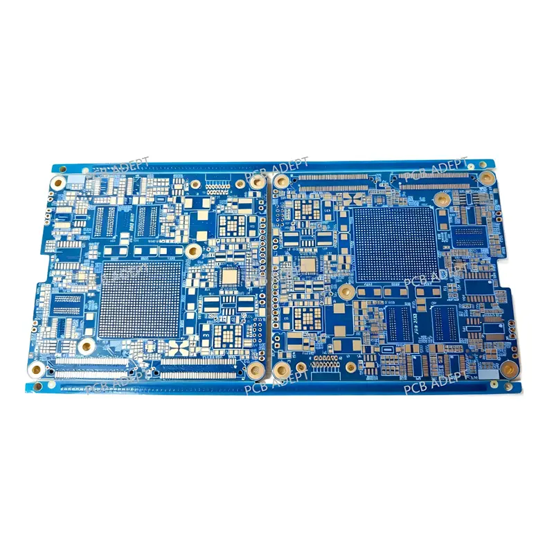
ODM High-Quality RF & Microwave PCBs for Mobile Phones and Radar Systems by China Suppliers and Factory - ≥500MHz Frequency Suppliers, Factory
Product Description
Never use ordinary FR-4. High-frequency dedicated boards with low loss and stable dielectric constant (such as Rogers RO4350B, RT/duroid series) must be selected. This is the cornerstone of performance.
Precise 50Ω impedance control is essential. Use microstrip lines, striplines or coplanar waveguides and determine the precise line width through calculation/simulation. When laying out, minimize the paths and avoid right angles.
Provide a complete and solid ground plane to ensure a low-impedance return path. Densely arrange grounding vias (especially on both sides of the transmission line) to suppress resonance and coupling.
Physically isolate the RF, digital, and power supply areas. When necessary, use shielding covers and via walls.
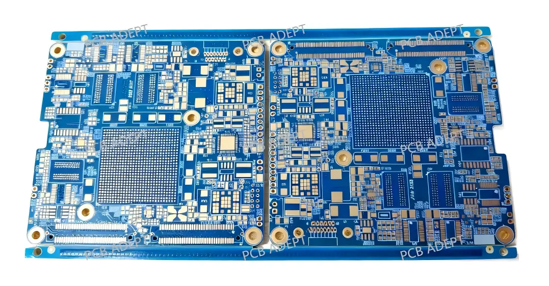
Strictly control the tolerance of line width and medium thickness to ensure signal integrity at high frequencies.
ENIG gold plating is preferred to ensure flatness and high-frequency conductivity for reliable RF performance.
The solder mask layer may affect the impedance, and "window opening" treatment is often adopted for RF traces.
RF PCBs play a very significant role in modern wireless communication devices, and an increasing number of customers are choosing such products.
RF & Microwave PCBs treat copper traces as transmission lines with controlled characteristic impedance, rather than simple electrical conductors. This requires specialized materials, precise geometries, and strict manufacturing tolerances that standard PCBs do not need.
FR-4 has a relatively high and unstable dielectric constant at high frequencies, along with higher signal loss (Df). These properties degrade signal integrity in RF applications. High-frequency laminates like Rogers RO4350B or RT/duroid series offer low loss and stable dielectric constants, which are critical for reliable RF performance.
50Ω is the industry-standard characteristic impedance for RF systems. Maintaining precise 50Ω impedance throughout the transmission lines ensures maximum power transfer and minimizes signal reflections, which is essential for maintaining signal integrity in high-frequency circuits.
ENIG provides an extremely flat and uniform surface, which is critical for consistent high-frequency signal transmission. The gold layer also offers excellent oxidation resistance and high-frequency conductivity, ensuring long-term reliability and stable electrical performance for RF traces and connectors.
RF & Microwave PCBs are widely used in wireless communication devices such as walkie-talkies, anti-drone equipment, electronic fence systems, radar systems, satellite communication equipment, 5G base stations, and various other modern wireless infrastructure products.
A complete and solid ground plane provides a low-impedance return path for RF signals, which is essential for minimizing noise and interference. Dense grounding vias placed on both sides of transmission lines suppress resonance and electromagnetic coupling between different circuit areas, significantly improving overall RF performance and signal isolation.









