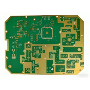
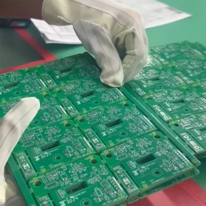
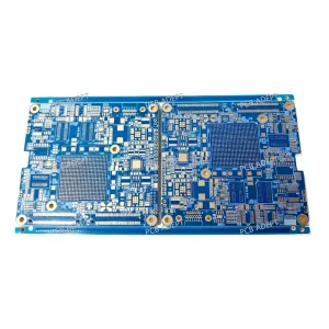
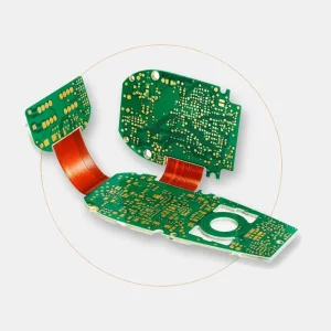
Featured High-Performance Circuit Solutions
Explore production-ready multilayer flex, rigid-flex, heavy copper, and thermal management architectures manufactured to rigorous global aerospace, automotive, and industrial benchmarks.
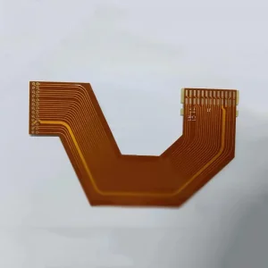
Multilayer Flexible Circuit Architecture & Engineering Physics
A rigorous examination of substrate material systems, interfacial shear stress mitigation, copper foil crystalline morphology, and laser blind/buried microvia processing.
Substrate Chemistry: Adhesiveless FCCL
Traditional multilayer flex circuits utilized modified acrylic or butyral-epoxy adhesive interlayers to bond copper foil to polyimide base films. However, these adhesives degrade thermal conductivity, introduce significant Z-axis thermal expansion (CTE mismatch), and reduce reliability during lead-free reflow (260°C peak). Premier fabrication facilities employ cast or laminated adhesiveless flexible copper clad laminates (FCCL) with thermoplastic polyimide or liquid crystal polymer (LCP). This significantly minimizes outgassing, preserves high insulation resistance, and provides superior mechanical fatigue endurance under continuous dynamic articulation.
Copper Metallurgy: RA vs. ED Copper
Determining the appropriate conductive foil crystalline microstructure dictates dynamic reliability. Rolled Annealed (RA) copper undergoes extensive longitudinal rolling and continuous annealing to create elongated, horizontal grain boundaries, permitting millions of cyclic bending deformations without micro-fracturing along grain planes. Conversely, Electrodeposited (ED) copper demonstrates columnar crystalline architecture oriented vertically, optimizing it for static "flex-to-install" applications where rigidity and fine-line etching resolution take precedence over repetitive deflection endurance.
Microvia & Lamination Dynamics
Fabricating high-density multilayer flexible PCBs (4 to 12+ layers) requires ultra-fast UV and CO2 laser ablation to produce blind and buried microvias down to 50 μm diameter. Controlled hydraulic vacuum lamination systems are calibrated with precision non-linear temperature ramps and pressure profiles to eliminate volatile void generation and resin starvation. Sequential buildup (SBU) processes ensure consistent dielectric thickness, enabling controlled single-ended (50Ω) and differential (90Ω/100Ω) impedance profiles with stringent tolerances.
Multilayer Flex PCB Quotation Dynamics & Cost Modeling
Understanding cost formation mechanisms, yield implications, and tooling parameters allows procurement engineers to negotiate favorable volume agreements without sacrificing structural integrity.
Layer Count & Stackup Complexity
Moving from a 2-layer FPC to a 4-layer, 6-layer, or 8-layer design increases processing steps exponentially. Each additional layer pair necessitates dedicated inner-layer etching, brown oxide treatments, AOI verification, and specialized adhesive/bonding film layers (polyimide or modified acrylic adhesive sheets). Complex book-binder designs or multi-opening flexible regions require multi-stage depth routing and customized lamination fixtures.
Coverlay vs. Solder Mask
Flexible solder masks (LPI) provide cost-effective insulation for moderate bending radii. However, for extreme dynamic flexing, polyimide coverlay (PI film pre-coated with thermo-setting adhesive) laminated under elevated heat and vacuum pressure is mandatory. Coverlay requires mechanical CNC punching or laser cutting of individual pad openings, driving NRE tooling fees and cycle time compared to photographic processing.
Surface Metallurgy & Finishes
The chosen surface finish directly influences cost, wire bonding compatibility, and contact life. While Electroless Nickel Immersion Gold (ENIG) is standard, ultra-thin gold or Immersion Silver is favored for dynamic flex joints to avoid nickel micro-cracking. For high-reliability gold-wire bonding or wiping contacts, Electroless Nickel Electroless Palladium Immersion Gold (ENEPIG) or thick Hard Gold (30-50 μinch) is quoted, incorporating high raw precious metal surcharges.
Stiffeners & Reinforcement
Multilayer flexible circuits inevitably incorporate localized mechanical stiffeners beneath SMT components, ZIF connectors, and strain-relief zones. Stiffener material choices—including FR-4, Polyimide (PI), stainless steel (SUS303/304), or aluminum backing—require selective 3M pressure-sensitive adhesives (PSA 467MP, 9077) or thermosetting epoxy bonding, which impact assembly hand labor and bill of materials.
Advanced Fabrication Capability Matrix: Multilayer Flexible PCBs
Comprehensive parameter specifications representing benchmark capabilities of top-tier Chinese manufacturing operations.
| Technical Parameter | Standard Commercial Capability | Advanced / Precision Limit | Quality Test & Verification Protocol |
|---|---|---|---|
| Layer Count Range | 1 – 6 Layers | 8 – 16 Layers (Rigid-Flex up to 26L) | Microsection cross-sectioning & optical microscopy |
| Base Copper Thickness | 1/3 oz (12 μm) / 1/2 oz (18 μm) | 1/4 oz (9 μm) to 2 oz (70 μm) | X-ray fluorescence (XRF) coating gauge |
| Minimum Line Width / Space | 0.075 mm / 0.075 mm (3 / 3 mil) | 0.025 mm / 0.025 mm (1 / 1 mil) via mSAP | Automated Optical Inspection (AOI) with AI classification |
| Laser Microvia Diameter | 0.10 mm (4 mil) | 0.05 mm (2 mil) UV Laser Drilled | High-resolution CT scanning & barrel integrity inspection |
| Controlled Impedance | ±10% Single-ended / Diff | ±5% Precision Impedance Match | Time Domain Reflectometry (TDR) test on coupon traces |
| Surface Finish Chemistry | ENIG (Au: 1-3 μ"), Immersion Tin | ENEPIG (Pd: 1-3 μ", Au: 2-4 μ"), Hard Gold | Gold thickness verification & solderability dipping test |
| Dielectric Film Materials | Kapton PI (12.5 μm, 25 μm, 50 μm) | Ultra-thin LCP, Upilex-S, Low-Dk PI | Dielectric Breakdown Voltage & Loss Tangent evaluation |
| Bending Endurance Radius | Static: 6x board thickness | Dynamic: 10x board thickness (>500k cycles) | Automated cyclic dynamic flexing endurance rig (MIT type) |
The China Manufacturing Ecosystem: Competitive Advantages
Analyzing the strategic supply chain consolidation, rapid NPI iteration, and massive technological capital investments that establish China as the premier manufacturing hub for advanced flexible circuits.
Aggregated Upstream Supply Chain
The Greater Bay Area (Shenzhen, Dongguan, Huizhou) hosts the world's most concentrated cluster of raw flex material suppliers. From domestic raw polyimide resin synthesis to tier-one global laminate suppliers (Panasonic, Shengyi, Rogers, Taiyo, DuPont), raw materials are sourced with minimal transit time. This localized ecosystem eliminates weeks of shipping latency for specialty FCCLs, conductive pastes, stiffener alloys, and bonding films, providing unbeatable agility for expedited NPI prototyping.
Automated Laser & Direct Imaging Capital
Modern Chinese tier-one and tier-two flex PCB factories have shifted away from manual contact printing and mechanical routing. Facilities feature automated cleanrooms equipped with Laser Direct Imaging (LDI) achieving 15μm resolution, roll-to-roll (R2R) horizontal desmear and chemical plating lines, and multi-beam UV/CO2 laser drilling systems. This automation dramatically reduces human handling, preventing crease damage, pinhole flaws, and substrate stretching on delicate 12.5μm PI layers.
Turnkey SMT & Box-Build Integration
Flex fabrication is rarely isolated. Handling ultra-thin multilayer flex during surface mount assembly (SMT) demands specialized magnetic pallet fixturing, low-temperature vacuum reflow, and precision robotic underfill dispensing. Chinese EMS leaders operate unified fabrication and SMT facilities under one roof. Sourcing bare boards and assembly through a single contract prevents finger-pointing between the board shop and the SMT house, maximizing product yield.
Macro Industry Solutions & Localized Application Scenarios
How multilayer flexible interconnects solve complex 3D routing, weight reduction, and signal integrity challenges across four dominant global industries.
Automotive EV Battery Management (BMS)
Modern electric vehicle (EV) battery packs are replacing heavy, failure-prone copper wire harnesses with integrated multilayer flexible circuits known as Cell Contact Systems (CCS). These 2-to-4 layer flex assemblies span meters in length, integrating voltage sensing lines, NTC thermistor sensor pads, and overcurrent fuses directly into a single ultra-light flat harness. This slashes pack assembly labor, saves crucial volumetric space, and guarantees continuous thermal performance under harsh automotive vibration.
Medical Diagnostics & Implantable Electronics
From disposable endoscopic camera probes to cochlear implants and smart wearable glucose monitors, medical devices require non-toxic, biocompatible flex circuits. Multilayer FPCs utilizing adhesiveless polyimide substrates and immersion pure gold finishes ensure zero cytotoxic outgassing. The extreme compactness allows 6 layers of wiring inside a 1.2mm catheter tip, routing high-definition digital sensor feeds through tight human anatomical pathways without signal attenuation.
Aerospace, Avionics & Defense Systems
Aerospace platforms operate under violent G-force shockwaves, vacuum conditions, and radical thermal swings (-65°C to +150°C). Multilayer flexible PCBs replace traditional pin-and-socket cable assemblies in radar gimbals, satellite solar panel deployment hinges, and missile seeker heads. Rigid-flex configurations eliminate human wire-crimping errors entirely, providing unified trace shielding against high-intensity radiated fields (HIRF) and lightning strikes.
Consumer Foldables & High-Speed IoT
Next-generation foldable smartphones, AR/VR headsets, and edge AI hardware require extreme dynamic bend fatigue life exceeding 200,000 hinge folding cycles. By employing ultra-thin modified polyimide (MPI) or Liquid Crystal Polymer (LCP) cores with rolled annealed copper placed strictly along the neutral bend axis, Chinese factories deliver 6-layer high-speed flex interconnects capable of transmitting PCIe Gen 4/5 and 28GHz mmWave RF signals seamlessly across moving mechanical hinges.
Global Procurement Strategy & Vendor Qualification Framework
A structured due-diligence audit protocol designed for procurement directors, quality assurance managers, and global supply chain strategists.
Stage 1: Engineering DFM Rigor
Before issuing tooling approvals, tier-one manufacturers execute automated DRC/DFM simulations. They analyze neutral axis stress vectors, trace transition fillets at stiffener boundaries, tear-drop reinforcements on all through-hole and via lands, and hatched ground planes for flexibility retention. Evaluating the depth and responsiveness of a factory's engineering feedback during quoting is the single most accurate predictor of downstream production yield.
Stage 2: Process Control & Traceability
Ensure the prospective partner operates under certified ISO 9001, IATF 16949 (for automotive), and ISO 13485 (for medical) quality management frameworks. Verify that individual panels carry unique 2D laser-etched DataMatrix codes. In premier Chinese facilities, this code syncs with the Manufacturing Execution System (MES), tracking every sub-process: lamination thermal profiles, copper plating current densities, etching speeds, and electrical test verification data.
Stage 3: Reliability & Destructive Testing
A credible factory must possess an internal analytical laboratory. Essential verification capabilities include: Cross-section micro-cleaving to verify copper plating thickness inside through-holes (>20μm minimum for IPC Class 3), Ionic Contamination testing (ROSE testing <1.56 μg/cm² NaCl equivalent), solder float thermal stress testing (288°C for 10 seconds, 3 cycles), and Peel Strength validation of the coverlay-to-copper bond.
Future Trends: The Next Decade of Flexible Electronics
Emerging fabrication disciplines reshaping multilayer flex: modified semi-additive processes (mSAP), embedded optics, and ultra-high frequency substrates.
Sub-20μm Ultra-Fine Pitch via mSAP
Subtractive etching reaches its physical limit at 35μm line/space due to trapezoidal undercut. Leading Chinese flex facilities are rapidly implementing Modified Semi-Additive Processes (mSAP). By utilizing ultra-thin copper seed foils (2-3μm) and pattern electroplating followed by micro-flash etching, engineers achieve vertical trace sidewalls with 15/15μm trace and spacing. This enables direct integration of 0.3mm pitch micro-BGA packages directly onto flexible substrate layers.
Liquid Crystal Polymer (LCP) Migration
As 5G/6G frequencies advance into the 30GHz-100GHz millimeter-wave spectrum, standard polyimide exhibits excessive dielectric loss (Df ~0.008) and high moisture absorption (~1.5%). Liquid Crystal Polymer (LCP) is emerging as the gold-standard substrate, offering an ultra-low Df (0.002), minimal water absorption (<0.04%), and hermetic sealing properties. Leading fabrication houses are mastering the narrow thermo-compression lamination window of LCP multilayer stacks for next-gen phased array antennas.
Embedded Passives & 3D Mechatronic Flex
The boundary between bare printed circuits and component packaging is blurring. Advanced flex development embeds thin-film resistors, planar inductors, and ceramic capacitors directly within inner flex dielectric cores. This eliminates external solder joints, frees up outer component real estate by 40%, and mitigates inductive parasitic loops, paving the way for hyper-miniaturized bio-implantable nodes and tactile robotic sensor skins.
Frequently Asked Engineering & Sourcing Questions
In-depth technical answers addressing the most critical design, validation, and commercial inquiries submitted by hardware designers and procurement specialists.
What is the fundamental difference between dynamic and static multilayer flex PCBs?
Static flex (flex-to-install) is designed to be bent or folded once during assembly and remain fixed throughout the operating lifespan of the product (e.g., folding inside an aerospace housing or an automotive dashboard). Dynamic flex, in contrast, must withstand continuous mechanical articulation, often spanning hundreds of thousands or millions of cycles (e.g., laptop display hinges, robotic joints, printhead cables). Dynamic multilayer flex mandates Rolled Annealed (RA) copper foils, adhesiveless polyimide substrates, balanced symmetrical stackups, and placing all critical copper traces precisely along the neutral mechanical bending axis.
How does moisture absorption in polyimide affect multilayer flex reflow soldering?
Polyimide is inherently hygroscopic, typically absorbing between 0.8% and 2.0% atmospheric moisture by weight depending on ambient humidity. If a multilayer flex circuit is exposed to standard assembly atmosphere and subjected directly to lead-free reflow temperatures (240°C–260°C), internal trapped water molecules undergo instantaneous vapor expansion. This leads to catastrophic internal delamination, coverlay blistering, and microvia barrel shear. Consequently, standard production protocol requires pre-baking all flex circuits at 105°C–120°C for 4 to 8 hours prior to SMT reflow, with assembly taking place within a strict 8-hour window.
What parameters must be included to obtain an accurate, immediate factory quote?
To avoid iterative estimation delays, a complete quote package should include: 1) Full Gerber RS-274X or ODB++ fabrication data; 2) Detailed stackup drawing clearly denoting individual core thicknesses, copper foil weights (RA or ED), and bonding adhesive sheets; 3) Exact stiffener material breakdown (FR4, PI, Aluminum, Stainless Steel) and adhesive type (PSA or Thermoset); 4) Desired surface finish (ENIG, ENEPIG, Hard Gold with thickness); 5) Controlled impedance callouts specifying layer, trace width, and reference planes; 6) IPC inspection class (Class 2 vs. Class 3); and 7) Panelization array drawing indicating fiducial and tooling hole locations.
Why is a hatched ground plane preferred over solid copper planes on flex layers?
Solid copper ground planes significantly compromise mechanical flexibility and increase the risk of substrate buckling, creasing, and delamination when bent around tight radii. Utilizing a 45-degree hatched ground plane (typically 50% to 70% copper coverage) reduces mechanical stiffness while maintaining sufficient electromagnetic interference (EMI) shielding. Furthermore, hatched designs allow outgassing volatiles from adhesive films to escape more readily during high-temperature vacuum lamination cycles, significantly improving inner-layer interfacial bond strength.
What causes tear propagation in flexible circuits and how is it engineered out?
Tear propagation typically initiates at sharp inside corners and mechanical transition slots when exposed to dynamic shear or handling stress. To eliminate tear hazards, modern DFM guidelines enforce: 1) Designing all inside corners with generous radii (minimum 1.5mm radius, preferably larger); 2) Incorporating sacrificial copper beads or teardrop trace reinforcement along all routed profile boundaries; 3) Utilizing punched circular stress-relief holes (minimum 3mm diameter) at the convergence point of internal slot cuts; and 4) Adding localized polyimide stiffeners spanning across bend-boundary transitions.
What standard lead times should be anticipated for multilayer flex prototypes and production?
Standard prototype manufacturing lead times for 4-to-8-layer multilayer flexible circuits generally range from 5 to 9 working days, depending on laser microvia count and stiffener complexity. Fast-turn prototype services in Shenzhen can compress this to 72–96 hours for high-priority NPI projects. High-volume mass production releases (10,000+ panels) typically operate on a 3 to 4-week production lead time, which accommodates rigorous incoming IQC, automated optical inspection, electrical flying probe or universal grid testing, and outgoing reliability compliance testing.
Advanced High-Reliability PCB & Assembly Portfolio
Explore specialized industrial options ranging from ultra-high frequency RF microwave substrates to ruggedized high-layer rigid-flex boards.