
1 / 2
ODM High Frequency PCB China Suppliers Factory - Minimize Signal Loss, EMI, Crosstalk & Impedance Mismatches Suppliers, Pricelist
Product Description
What is High Frequency PCB?
Definition
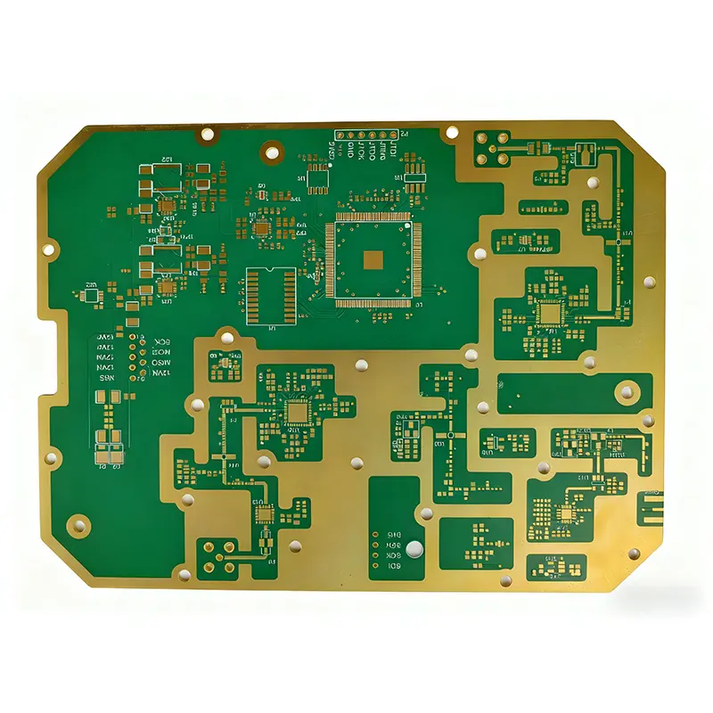
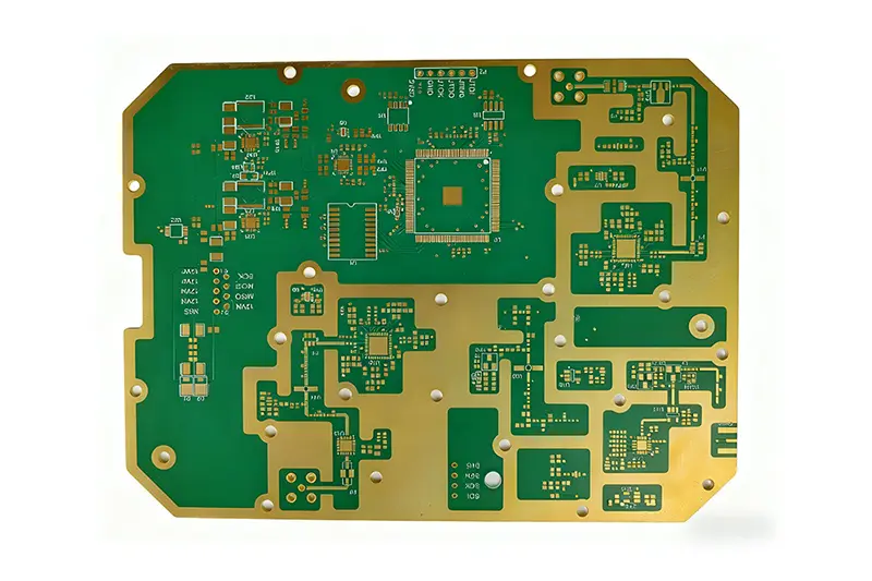
High-frequency PCBs are special printed circuit boards specifically designed to handle high-frequency signals (typically referring to frequencies above 500MHz or digital signal rise times less than 1 nanosecond).
Main Application Fields
-
📡Communication Infrastructure Antennas, power amplifiers, filters, and low-noise amplifiers for 5G/6G base stations.
-
🚗Automotive Electronics Millimeter-wave radar, advanced driver assistance systems, in-vehicle satellite communication.
-
✈️Aerospace & Defense Radar systems, electronic warfare equipment, satellite communication terminals, seeker heads.
-
💻High-Speed Computing & Data Comm High-speed server/router backplanes, optical modules, 400G/800G switches.
-
🔬Test & Measurement Instruments Network analyzer, high-frequency oscilloscope, signal source.
Core Material Selection Principles
High-frequency signals are easily affected by the dielectric properties and losses of the substrate. Material selection is the core of high-frequency PCBs.
| Material Type | Key Parameters | Recommended Material / Specification | Applicable Scene |
|---|---|---|---|
| Base Material |
• Dielectric constant (Dk) • Dielectric loss tangent (Df) • Coefficient of thermal expansion (CTE) |
High-frequency dedicated substrate: • PTFE (polytetrafluoroethylene, Dk=2.1–2.6, Df≤0.0009) • Rogers series (e.g. RO4350B, Dk=3.48, Df=0.0037) • Modified epoxy resin (FR-4 high-frequency version, Dk=3.8–4.2, Df≤0.01) |
PTFE/Rogers: Millimeter wave, radar, 5G base station High-frequency FR-4: Consumer electronics (mobile phones, routers) |
| Copper Foil | Surface roughness | Low profile copper foil (LP) / very low profile copper foil (VLP), roughness ≤1.0μm | Reduce transmission loss on copper foil surface (skin effect) |
| Solder Mask Layer | Dielectric loss | High-frequency special solder mask oil (Df≤0.01) | Avoid increasing signal attenuation from the solder mask layer |
Key Design Points
Precise Impedance Control
- High-frequency PCBs must control characteristic impedance (e.g. 50Ω single-ended, 100Ω differential), with deviation ≤±5% (vs. ±10% for standard PCBs).
- Impedance calculation requires combining base material Dk, plate thickness, line width/spacing, and copper foil thickness — simulate with professional software (e.g. Polar SI9000).
- Example: RO4350B substrate (thickness 0.254mm) — a 50Ω single-ended impedance corresponds to approximately 0.8mm line width.
- Impedance compensation: Reserve ±0.02mm line width compensation for etching side etching and solder mask coverage effects.
Routing Optimization
- Traces should be as short and straight as possible — avoid right angles or acute angles (prone to reflection at high frequencies); fillet radius ≥0.5mm.
- Differential traces must be equal in length and spacing (length difference ≤5mil) with ground wrapping (ground-to-differential distance ≤2× line width) to reduce EMI.
- Skin effect response: High-frequency current concentrates on copper foil surface — use silver-plated copper foil (to reduce surface resistance) or widen traces (to reduce current density).
Grounding and Shielding Design
- Complete ground layer (GND Plane) is required — avoid ground layer segmentation; keep signal-to-ground layer distance ≤0.2mm to enhance coupling and reduce impedance.
- For sensitive RF areas (e.g. RF chips), design metal shielding covers with reliable grounding (multiple grounding points, spacing ≤λ/20).
- High-frequency devices (e.g. power amplifiers) generate significant heat — design heat dissipation pads and metallized via arrays (via diameter ≥0.3mm, spacing ≤1mm).
- Prioritize miniaturized, low-parasitic packaging (e.g. QFN, LGA) to reduce signal reflections from packaging.
Manufacturing Process Control
Precision Control
- Line width/spacing tolerance: ≤±0.01mm (vs. ±0.02mm for standard PCBs) — using high-precision Laser Direct Imaging (LDI) technology instead of traditional film exposure.
- Lamination accuracy: Interlayer alignment deviation ≤0.02mm to avoid impedance offset; bonding temperature and pressure must match base material characteristics (PTFE requires high-temperature, high-pressure bonding).
Loss Control
- Etching process: Micro-etching technology reduces copper foil surface roughness and avoids increased transmission loss; lateral erosion ≤0.01mm.
- Surface treatment: Prefer Electroless Nickel Immersion Gold (ENIG) or silver plating over OSP (organic film increases contact resistance); gold layer thickness ≤0.1μm (excessive thickness increases loss).
⚡ Core Summary: The essence of high-frequency PCBs lies in "reducing signal loss, ensuring precise impedance, and minimizing electromagnetic interference". This requires full-process control from low-loss substrate selection → precise impedance design → high-precision manufacturing. For different high-frequency scenarios (e.g. 1GHz vs. 60GHz), substrate and process parameters must be specifically adjusted.
Send Inquiry
Frequently Asked Questions (FAQ)
Q What is the difference between a high-frequency PCB and a standard FR-4 PCB?
High-frequency PCBs use specialized substrates (such as PTFE or Rogers materials) with significantly lower dielectric constants (Dk) and dielectric loss tangents (Df) compared to standard FR-4. This allows them to handle signals above 500MHz with minimal signal loss and distortion, whereas standard FR-4 boards are typically suitable for lower-frequency applications below 1GHz.
Q What materials are most commonly used for high-frequency PCBs?
The most commonly used materials include PTFE (polytetrafluoroethylene) with Dk=2.1–2.6 and Df≤0.0009, Rogers series laminates such as RO4350B (Dk=3.48, Df=0.0037), and high-frequency versions of modified epoxy resin (FR-4 high-frequency grade, Dk=3.8–4.2). The choice depends on the operating frequency, application environment, and cost requirements.
Q Why is impedance control so critical in high-frequency PCB design?
At high frequencies, any impedance mismatch along signal traces causes signal reflections, which degrade signal integrity and increase electromagnetic interference (EMI). High-frequency PCBs typically require characteristic impedance control within ±5% tolerance (e.g. 50Ω single-ended or 100Ω differential), compared to ±10% for standard PCBs, to ensure reliable signal transmission.
Q What industries most commonly use high-frequency PCBs?
High-frequency PCBs are widely used across 5G/6G communication infrastructure, automotive millimeter-wave radar and ADAS systems, aerospace and defense radar and electronic warfare equipment, high-speed computing (400G/800G data centers), and precision test and measurement instruments such as network analyzers and high-frequency oscilloscopes.
Q What surface finish is recommended for high-frequency PCBs?
Electroless Nickel Immersion Gold (ENIG) or silver plating is strongly preferred for high-frequency PCBs. OSP (Organic Solderability Preservative) is generally avoided because the organic film increases contact resistance. The gold layer thickness should be kept at ≤0.1μm, as excessive thickness can increase signal loss at high frequencies.
Q How does the manufacturing process for high-frequency PCBs differ from standard PCBs?
High-frequency PCB manufacturing requires significantly tighter tolerances: line width/spacing tolerance ≤±0.01mm (vs. ±0.02mm for standard), interlayer alignment deviation ≤0.02mm, and micro-etching technology to minimize copper foil surface roughness. Laser Direct Imaging (LDI) replaces traditional film exposure for greater precision, and special high-temperature/high-pressure lamination processes are required for PTFE-based substrates.









