
China Heavy Copper PCB for Power Converters - China Suppliers & Factory with Strong Current-Carrying Capacity and Heat Dissipation Manufacturers, Factories
Product Description
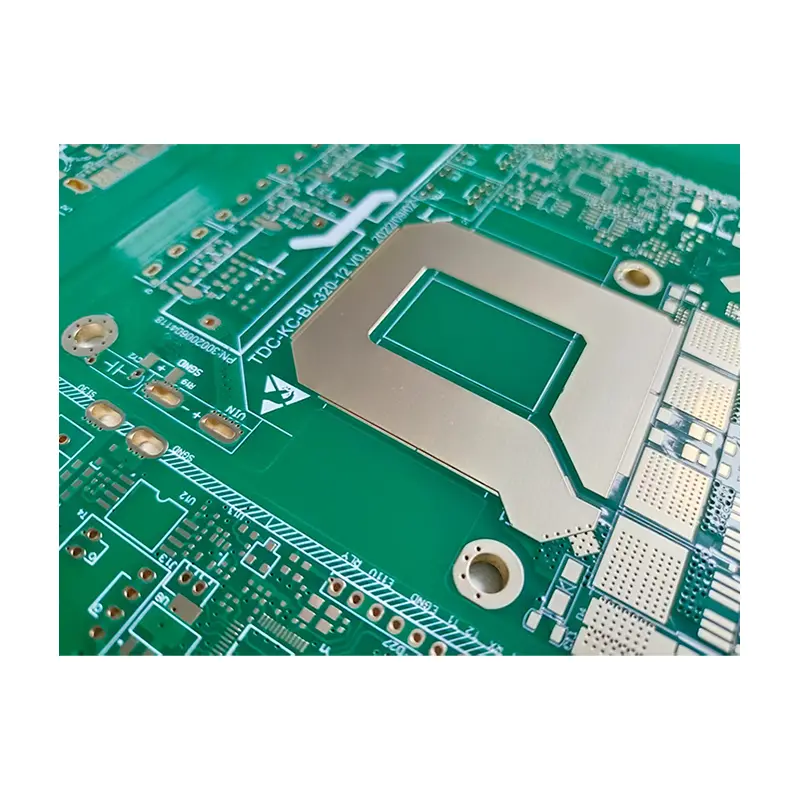
What is Heavy Copper PCB?
The core is used in high-current and high-power scenarios (such as power supplies, new energy, industrial control, etc.). The key points of its design, manufacturing and application are as follows:
Core Features and Application Scenarios
• Good heat dissipation: The thick copper layer can quickly conduct heat, reducing the risk of overheating of the device.
• High mechanical strength: Thick copper enhances the PCB's resistance to bending and impact.
Key Design Points
- Common specifications: 70μm (2 ounces), 105μm (3 ounces), 140μm (4 ounces), and up to 420μm (12 ounces) in extreme scenarios.
- Matching scenarios: For large current (≥5A) circuits, 2 to 4 ounces of copper should be preferred. For ultra-power scenarios (≥20A), 6 to 12 ounces of copper should be selected.
- Current-carrying capacity calculation: Combined with copper thickness, line width, and temperature rise requirements (usually designed based on a temperature rise of 10℃). Formula reference: \(I = K \times W \times T^{0.83}\) (I is current, K is coefficient, W is line width, T is copper thickness). Example: 2 oz copper (70μm), width 5mm, carrying capacity ~15A (10℃ rise).
- Trace optimization: Keep high-current traces as short and wide as possible. Multi-layer boards can adopt "parallel connection of multiple layers of copper foil".
- Vias: Increase hole diameter (≥0.5mm) and number of vias (estimated at 1A per hole). Copper plating thickness on the hole wall should be ≥20μm.
- Pads: Thick copper pads need to be enlarged (0.2 to 0.5mm larger than ordinary pads) to prevent rapid heat dissipation during welding, avoiding false soldering.
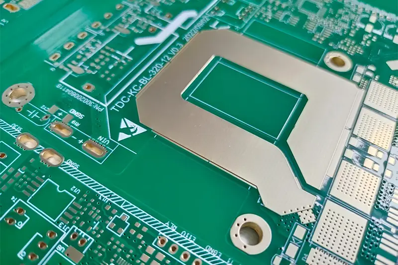
- Heat dissipation: Design thick copper areas as "copper sheet heat sinks", or add metallized via arrays (spacing ≤1mm) connecting to the heat dissipation layer.
- Insulation: Widen wire spacing for thick copper layers (for 70μm copper, spacing should be ≥0.2mm) to prevent creepage breakdown under high voltage.
Manufacturing Process Difficulties and Control
- Thick copper lamination: High-temperature and high-pressure lamination (180℃/4MPa) is required to ensure peel strength between copper foil and substrate (≥1.2N/mm).
- Thick copper etching: Etching rate is slow (~1μm/min). Etching time must be controlled to avoid side etching (amount ≤0.05mm). A stepwise etching process should be adopted.
The CTE of thick copper layers differs significantly from that of the substrate. When laminating, a "symmetrical structure" (consistent copper thickness between upper and lower layers) must be adopted, and a rigid support layer added to prevent warping (warping degree ≤0.5%).
The surface of thick copper is prone to oxidation. Prefer tin plating (high-temperature tin layer) or nickel-gold plating to avoid OSP. Enlarged "solder mask opening windows" are needed in the pad area to ensure bonding force.
Core Summary
The core of heavy copper PCBs is "high current carrying capacity + heat dissipation". In terms of design, it is necessary to match the copper thickness and current carrying capacity requirements. In manufacturing, problems such as thick copper etching and lamination warping need to be solved. They are suitable for high-power and high-current industrial and energy scenarios.









