
1 / 1
Famous High-Quality Heavy Copper PCBs from China Suppliers - Ideal for Power Converters and Vehicles with Superior Heat Dissipation Supplier, Pricelist
Product Description
What is Heavy Copper PCB?
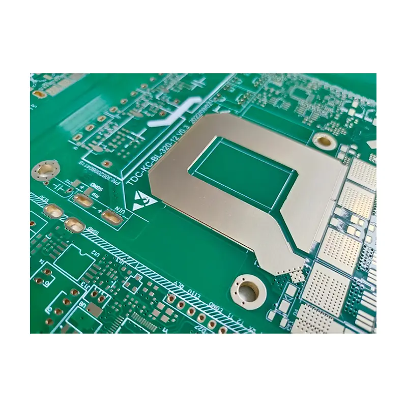
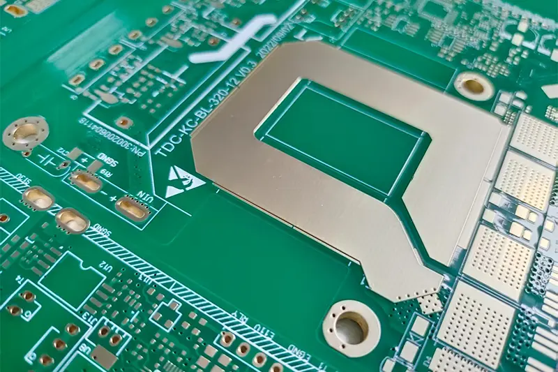
▶Heavy copper PCBs are predominantly utilized in high-current and high-power applications (such as power supplies, new energy vehicles, industrial control systems, and renewable energy equipment). The core engineering principles, production complexities, and application scenarios are outlined below.
Core Features and Application Scenarios
⚡
Strong Current-Carrying Capacity
The current-carrying capacity of 70μm copper foil (2 oz) is approximately double that of 35μm copper foil (1 oz) under identical trace width specifications.
🌡️
Superior Heat Dissipation
Heavy copper layers conduct thermal energy rapidly into heat sink paths, significantly lowering operating temperatures and component stress.
🔩
High Mechanical Strength
Thickened copper cladding reinforces board stiffness, dramatically improving resistance to thermal cycling, vibration, and mechanical impact.
Typical Applications
Power converters (AC-DC / DC-DC), Battery Management Systems (BMS) for electric vehicles, industrial frequency inverters, welding machine control modules, and solar power converters.
Key Design Points
1
Selection of Copper Foil Thickness
- Standard Heavy Specifications: 70μm (2 oz), 105μm (3 oz), 140μm (4 oz), with specialized configurations reaching up to 420μm (12 oz).
- High-Current Circuits (≥5A): Recommended standard selection is 2 oz to 4 oz copper.
- Ultra-Power Scenarios (≥20A): Recommended selection is 6 oz to 12 oz copper foil.
2
Trace and Current-Carrying Capacity Optimization
Current Capacity Calculations:
- Design calculations balance copper thickness, trace width, and thermal limits (standard target: ≤10℃ temperature rise).
- Calculation Formula: I = K × W × T0.83 (where I = current, K = derating coefficient, W = trace width, T = copper thickness).
- Design Benchmark: A 2 oz (70μm) trace with a 5mm width supports approximately 15A at a 10℃ temperature rise.
- Route power conductors with minimal lengths and maximal width, strictly avoiding sudden trace narrowing (neck-downs) to prevent localized thermal hotspots.
- Multi-layer constructions can parallelize copper planes across adjacent layers (e.g., dual parallel 2 oz layers yielding 4 oz capacity).
3
Via and Soldering Pad Specifications
- Vias: Enlarge via drill diameters (≥0.5mm), utilize via arrays (calibrated at ~1A current transfer per via), and enforce hole-wall copper plating of ≥20μm (compared to 8–12μm for standard PCBs).
- Pads: Enlarge heavy copper surface-mount and through-hole pads by 0.2–0.5mm beyond standard library dimensions to counteract thermal dissipation during soldering and eliminate cold solder joints.
4
Thermal Dissipation and Dielectric Clearance
- Thermal Dissipation: Implement direct-pour heavy copper thermal planes or stitch via matrices (pitch ≤1.0mm) bridging directly into dedicated dissipation heat spreaders.
- Dielectric Isolation: Enlarge trace-to-trace spacing (e.g., minimum spacing ≥0.2mm for 70μm copper) to eliminate high-voltage creepage and breakdown hazards.
Manufacturing Challenges & Process Controls
▶ 1. Heavy Copper Lamination and Chemical Etching
Lamination Adhesion: Demands strictly controlled elevated temperature and pressure cycles (180℃ / 4MPa) to guarantee foil peel strength ≥1.2N/mm.
Subtractive Etching: Thicker copper significantly decreases etch speed (~1μm/min). Etch cycles require compensation modeling and specialized multi-stage etching chemistry to suppress lateral side-undercutting (lateral undercut target ≤0.05mm).
Subtractive Etching: Thicker copper significantly decreases etch speed (~1μm/min). Etch cycles require compensation modeling and specialized multi-stage etching chemistry to suppress lateral side-undercutting (lateral undercut target ≤0.05mm).
▶ 2. Lamination Symmetry & Warpage Mitigation
Because thick copper foils exhibit a substantial Coefficient of Thermal Expansion (CTE) differential compared to dielectric resin substrates, panel layups must utilize strict symmetrical core/prepreg distribution and balanced copper distributions to restrict total board bow and twist to ≤0.5%.
▶ 3. Surface Finishes and Solder Mask Application
Heavier copper runs have increased oxidation surface area. Recommended surface finishes include Immersion Tin or Electroless Nickel Immersion Gold (ENIG) over OSP to ensure full boundary sealing.
Additionally, enlarged solder mask relief apertures are mandated to facilitate deep resin penetration around high-profile trace step walls.
Additionally, enlarged solder mask relief apertures are mandated to facilitate deep resin penetration around high-profile trace step walls.
Engineering Summary
💡
The fundamental value of heavy copper printed circuit boards centers on high current-carrying capacity coupled with superior thermal conduction. Successful deployments require rigorous alignment between copper cross-sectional area and thermal limits during design, combined with strict multi-step etch compensation and structural warpage control during manufacturing.
Request Technical Consultation & Quote
Frequently Asked Questions
Q1
What is considered "heavy copper" in PCB manufacturing?
Heavy copper PCBs are defined as printed circuit boards containing conductor thicknesses of 3 oz/ft² (105μm) or greater on either outer or inner layers. Standard PCBs conventionally use 1 oz (35μm) copper. Standard production selections include 2 oz, 3 oz, and 4 oz, reaching up to 12 oz (420μm) for extreme power management hardware.
Q2
What are the main advantages of using heavy copper PCBs?
Heavy copper PCBs provide three core engineering advantages: (1) Enhanced Current Capacity: Enables elevated electrical loads without widening traces excessively; (2) Superior Thermal Dissipation: Directly sinks heat from components to planes and external coolers; and (3) Mechanical Endurance: Significantly boosts physical strength across thermal stress cycles and vibration environments.
Q3
In which industries and applications are heavy copper PCBs most commonly used?
Heavy copper technology is widely deployed in high-load power conversion systems (AC-DC and DC-DC), Electric Vehicle Battery Management Systems (BMS), industrial variable-frequency drives, power grid switching systems, automated welding equipment, renewable solar/wind inverters, and aerospace electrical distribution boards.
Q4
How do I calculate the current-carrying capacity of a heavy copper trace?
Current handling capacity is determined using IPC-2152 standard calculations or the baseline formula: I = K × W × T0.83 (where I = current in amperes, K = environmental derating factor, W = conductor width, and T = foil thickness). For instance, a 2 oz (70μm) trace measuring 5mm in width safely handles approximately 15A with a 10℃ permissible temperature rise.
Q5
What manufacturing challenges are unique to heavy copper PCBs?
Key manufacturing hurdles include: (1) Etch Undercutting: Extended chemical exposure requires step-etch methods to protect critical trace geometries; (2) CTE-Induced Warpage: Significant thermal mismatch demands balanced resin/copper symmetry; and (3) Resin Void Elimination: Filling tall trace gaps requires high-flow prepregs and precision vacuum lamination.
Q6
How should vias and pads be designed in a heavy copper PCB for high-current applications?
High-current via design requires drill diameters of ≥0.5mm, hole-wall copper plating of ≥20μm (substantially higher than the standard 8–12μm baseline), and parallel via arrays sized around 1A per via. Solder pads should be expanded by 0.2–0.5mm over standard footprint sizes to preserve thermal energy during assembly and prevent cold solder joints.









