
Featured OEM PCB Manufacturing Solutions
Explore our flagship OEM & ODM circuit boards engineered for robust thermal dissipation, millimeter-wave radio frequencies, high current density, and harsh operating environments.

China Heavy Copper PCB for Power Converters - China Suppliers' Superior Factory Products for Enhanced Heat Dissipation and Current Capacity Supplier, Pricelist
View Product Details
ODM High-Frequency RF & Microwave PCBs from China Suppliers - Low Loss, Excellent Signal, Impedance Control ≥500MHz Factory Solutions Suppliers, Company
View Product Details
ODM China Raspberry Pi HAT Suppliers: Affordable Factory Solutions for Learning and IoT Projects Companies, Pricelist
View Product Details
Buy High-Quality Heavy Copper PCBs from China Factory: Ideal for Power Converters and Strong Current Applications – Top Suppliers Company, Factory
View Product Details
ODM China Rigid Flex PCB Suppliers - Single & Double-Sided Rigid Flex/4-16 Layer Multi-Layer PCB Factory Quotes, Factory
View Product Details
OEM High Thermal Conductivity Aluminum PCB from China Suppliers - Reliable Factory for Custom Solutions Factories, Factory
View Product Details
Buy China Flexible PCB Suppliers - Lightweight & Bendable Solutions from a Leading Factory for Consumer Electronics Manufacturer, Factories
View Product Details
OEM High-Quality Rigid Flex PCB from China Suppliers | Custom 4-16 Layer Multi-Layer PCB Factory Manufacturer, Factories
View Product DetailsEngineering Scalability in PCB Manufacturing: Macro Industry Solutions
Modern hardware development demands far more than basic trace etching. High-performance computing, automotive electrification, and defense-grade communications dictate uncompromising precision, material integrity, and automated process controls.
Thermal Dissipation & Power Density
As silicon modules compress gigawatts into micro-footprints, PCB substrate thermal resistance becomes the ultimate bottleneck. Our heavy copper substrates (up to 12 oz) and high-thermal-conductivity metal-core aluminum boards (up to 5.0 W/m·K) dissipate heat directly away from switching MOSFETs and power ICs, eliminating hotspots in energy storage systems and industrial motor drives.
- Heavy copper up to 12 oz copper thickness
- Aluminum and copper core thermal conductivity up to 5 W/m-K
- Direct thermal vias with conductive resin plugging
High-Frequency Signal Integrity (≥500MHz to 77GHz)
High-speed edge devices, millimeter-wave radar, and 5G/6G RF nodes experience severe dielectric attenuation and skin-effect dispersion. We deploy PTFE-based Rogers, Taconic, and Nelco laminates with tight dielectric constant (Dk 2.2 to 3.5) tolerance and ultra-low loss tangent (Df ≤0.0015), matched with precision-controlled impedance routing within ±5%.
- Controlled impedance within ±5% precision tolerance
- Hybrid pressing: Rogers/Taconic PTFE bonded with FR4
- ENEPIG & hard gold surface finishes for minimal RF loss
Miniaturization & 3D Rigid-Flex Packaging
Wearable diagnostics, defense optics, and unmanned aerial systems cannot accommodate bulky wire harnesses and heavy sheet enclosures. Our multi-layer rigid-flex solutions (up to 22 layers) combine dynamic bendability with dense SMT zones, reducing interconnect resistance, eliminating crimp connectors, and slashing mechanical assembly weight by up to 60%.
- Polyimide (PI) flexible cores with teardrop copper fillets
- Laser-cut stiffeners in stainless steel, FR4, and aluminum
- Multiple bending radius qualification: >100,000 flex cycles
Technology Roadmap: Next-Generation PCB Manufacturing
As semiconductor nodes shrink to sub-3nm, printed circuit board fabrication transitions from macro-machining to nanoscale chemical and laser micro-engineering. Our roadmap charts the progression across line-width reduction, HDI microvias, and advanced substrate-like architectures.
Phase 1: Sub-35µm SAP & mSAP
Replacing conventional subtractive etching with Modified Semi-Additive Processes (mSAP). Enables straight trace sidewalls, ultra-sharp rectangular geometries, and line/space geometries down to 30/30µm for ultra-dense BGA pitch breakouts below 0.35mm.
Commercial ProductionPhase 2: Any-Layer HDI & Microvias
Ultra-short laser drilled microvias (CO2 and UV laser ablation) filled with electroplated copper (VIPPO). Eliminates capacitive stubs in multi-gigabit routing, enabling seamless blind/buried via interconnects through any layer without signal bounce or parasitic losses.
Mass Production ActivePhase 3: Substrate-Like PCB (SLP)
Bridging the gap between conventional PCBs and IC packaging substrates. Employing thin-core dielectric laminates and photo-imageable solder masks, achieving 20/20µm trace resolution to integrate heterogeneous system-in-package (SiP) modules for AI edge hardware.
Engineering ValidationPhase 4: Embedded Silicon & Passives
Embedding capacitors, inductors, and bare silicon dies directly within internal PCB core layers. Frees surface footprint for fine-pitch BGAs, drastically curtails loop inductance to under 0.1 nH, and maximizes thermal conduction across high-power switching matrices.
R&D Pilot Lines| Manufacturing Parameter | Standard Capability | Advanced Capability (High-Density / RF) | Quality Verification Protocol |
|---|---|---|---|
| Layer Count | 1 – 8 Layers (FR4, CEM-1) | Up to 32 Layers (Hybrid, Rigid-Flex, High TG) | Cross-sectioning & Metallurgical X-Ray |
| Minimum Line Width / Spacing | 3.5 mil / 3.5 mil (0.088mm) | 1.8 mil / 1.8 mil (0.045mm via mSAP) | Automated Optical Inspection (AOI) |
| Base Copper Thickness | 0.5 oz – 2 oz (18µm – 70µm) | 3 oz – 12 oz (Extreme Heavy Copper) | Micro-resistance Eddy Current Meters |
| Laser Microvia Aspect Ratio | 0.8:1 | 1:1 Stacked & Staggered Microvias | 3D X-Ray Inspection (AXI) |
| Dielectric Constant (Dk) | 4.2 – 4.8 (Standard FR-4) | 2.1 – 3.5 (Rogers, Taconic, PTFE) | Vector Network Analyzer (TDR / VNA) |
| SMT Placement Resolution | 0201 passives, 0.4mm pitch BGA | 01005 passives, 0.3mm pitch BGA / CSP | Inline 3D Solder Paste Inspection (SPI) |
China Factory 4.0: Supply Chain Resilience & Efficiency
Shenzhen is the world’s electronics nexus—home to Huawei, BYD, and DJI. Operating inside our 8,000 m² state-of-the-art facility in Bao'an District, Shenzhen ICSLOVE Technology integrates end-to-end cyber-physical systems to shorten prototyping cycles and eliminate supply chain blind spots.
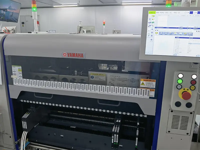
YAMAHA High-Speed SMT
6 high-speed SMT lines handling 01005 passives and ultra-fine pitch BGAs with micron-grade placement accuracy.
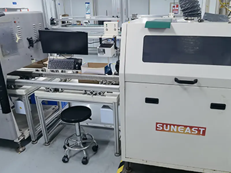
Dual-Stage Optical Inspection
Pre-reflow and post-reflow 3D AOI intercepts component shifts, polarity reversals, and micro-bridging instantaneously.
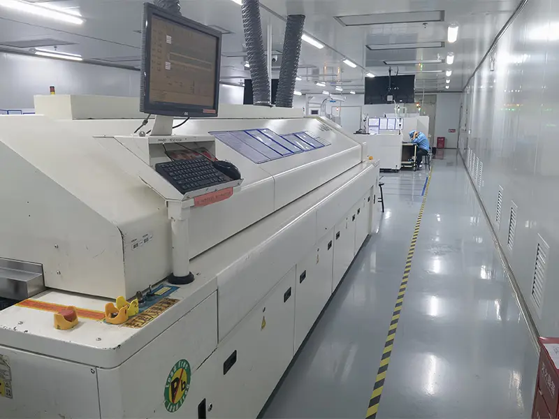
Multi-Zone Lead-Free Reflow
10-zone nitrogen-purged reflow ovens customized with product-specific thermal recipes to prevent pad voiding.
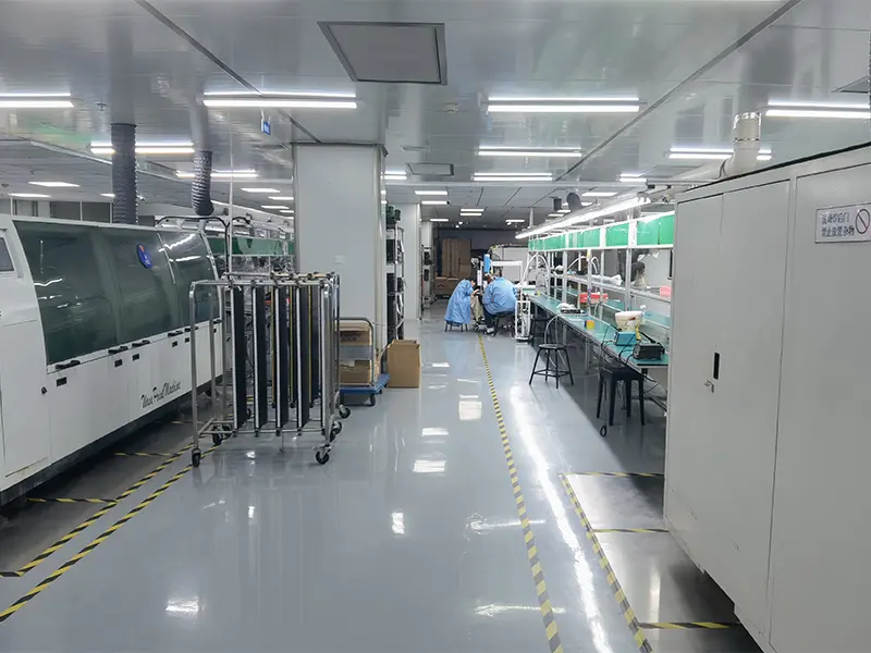
DIP & Selective Wave Soldering
4 specialized DIP lines dedicated to high-amperage terminal blocks, transformers, and ruggedized through-hole joints.
MES End-to-End Traceability
Our cloud-interfaced Manufacturing Execution System (MES) assigns an indelible 2D DataMatrix code to every single PCB board. From raw laminate batch numbers and solder paste temperature to feeder lot codes, reflow thermal curves, and AOI inspection images, every variable is archived for 10 years to support aerospace and medical audit trails.
Sub-48-Hour Component Kitting
Located at the epicenter of Huaqiangbei and Pearl River Delta distribution hubs, our procurement network accesses direct factory reels of Texas Instruments, Analog Devices, STMicroelectronics, Microchip, and Murata within hours. By mitigating broker markups and counterfeit risks, overseas OEMs secure tier-1 pricing and fast turnover.
Agile Prototype to Volume Scaling
Overseas clients commonly face a frustrating chasm between agile prototyping labs and massive contract manufacturers who reject sub-10,000-piece orders. We eliminate this friction: our dedicated fast-track prototype cells fabricate and assemble 1 to 500 units in 3 to 9 days, subsequently scaling into mass runs on automated lines without engineering re-qualification.
Global Enterprise Procurement Demands & Strategic Sourcing
Strategic supply chain managers demand transparency, total landed cost predictability, and zero single-point failure risks. Here is how our comprehensive DFM, BOM optimization, and component verification framework protects engineering budgets.
DFM, DFA & DFT Pre-Production Audits
Before copper clad laminates enter our CNC routers, our CAM engineering squad runs complete automated Design for Manufacturability (DFM), Design for Assembly (DFA), and Design for Test (DFT) scrubs. We identify aspect ratio violations, solder mask slivers below 3 mil, component shadow zones during reflow, and un-testable net stubs before you spend a single dollar on tooling.
BOM Scrubbing & 10%+ Cost-Down Engineering
Single-sourced components create catastrophic supply bottlenecks. Our component engineering department actively reviews your Bill of Materials (BOM) to suggest drop-in pin-compatible alternates for long-lead passives, crystal oscillators, and standard logic ICs. We achieve an average 10% to 22% bill-of-materials cost reduction while insulating your line from sudden market shortages.
Rigorous Anti-Counterfeit IQC Inspection
Counterfeit silicon ruins brands. Every passive and active component entering our facility undergoes a strict Incoming Quality Control (IQC) protocol: microscopic package laser markings inspection, decapsulation die verification under high magnification, pin-finish X-ray fluorescence (XRF) testing for RoHS compliance, and moisture sensitivity level (MSL) baking prior to vacuum packing.
Trusted By Leading Electronics & Engineering Brands Worldwide





Localized Global Support & Regulatory Compliance
International hardware developers must navigate stringent safety, environmental, and electro-magnetic compatibility hurdles. We maintain a zero-compromise compliance matrix ensuring seamless entry into North American, European, and Asia-Pacific markets.
IPC-A-610 / 600 Class 2 & Class 3
Production lines operate under strict IPC Class 2 (consumer/industrial) and IPC Class 3 (high-reliability, mission-critical aerospace/defense). We enforce minimum annular ring geometries, copper barrel plating thickness (>25µm), and rigorous solder joint wetting requirements.
ISO 9001 & IATF 16949 Standards
Our quality management system is audited under ISO 9001:2015. Automotive lines mirror IATF 16949 methodologies including APQP (Advanced Product Quality Planning), PPAP (Production Part Approval Process), and FMEA failure mode analysis to assure near-zero defect ppm levels.
UL 94V-0, RoHS 3 & REACH Compliant
All raw copper-clad laminates, prepregs, solder masks, and fluxes carry authentic UL 94V-0 flammability ratings. Fully compliant with EU Directive 2015/863 (RoHS 3) lead-free mandates, SVHC REACH guidelines, and Dodd-Frank Act conflict-free mineral sourcing policies.
Need Full Turnkey Box Build & Mechanical Integration?
Beyond bare PCB fabrication and SMT/DIP assembly, our Bao'an facility provides CNC rapid tooling, plastic enclosure injection molding, conformal coating, custom cable harnessing, MCU flashing, and final consumer packaging.
Frequently Asked Questions: OEM PCB Manufacturing
Get authoritative technical answers regarding fabrication tolerances, assembly lead times, intellectual property protection, and quality certification.
What files are strictly required to initiate a turnkey PCB manufacturing and PCBA quote?
How does PCB ADEPT guarantee component authenticity and prevent counterfeit parts?
What are the lead times for fast-turn prototype fabrication versus mass production?
Can your factory fabricate high-frequency hybrid PCB stack-ups with Rogers and FR4?
How is intellectual property (IP) and proprietary firmware protected during production?
What testing methodologies are implemented before final shipment?
Advanced OEM & ODM PCB Solutions
Review our extensive range of high TG boards, flexible circuits, Raspberry Pi HATs, and fast-turn validation prototypes configured for modern electronics developers.
High-Quality China Rigid Flex PCB Suppliers | Single & Double-Sided, Multi-Layer Rigid Flex PCB Factory Manufacturers, Quotes
View Product Details
ODM High Frequency PCB China Suppliers Factory - Minimize Signal Loss, EMI, Crosstalk & Impedance Mismatches Suppliers, Pricelist
View Product Details
High-Quality China PCB Prototype: Rapid Prototyping and Validation by Leading Suppliers and Factory for Modern Electronics Pricelist, Factories
View Product Details
Famous High-Quality Rigid Flex PCB from China Factory - Single & Double-Sided, 4-16 Layer Suppliers Quotes, Factory
View Product Details
Famous High Thermal Conductivity Aluminum PCB from China Suppliers and Factory - Ideal for Your Electronics Needs Companies, Factories
View Product Details
China High TG PCBs for Automotive, Aerospace & Defense | China Suppliers & Factory for TG150, TG170, TG180, TG260, TG300 Quotes, Pricelist
View Product Details
Famous Raspberry Pi HAT from China Factory: Top Suppliers for Mini Single-Board Computer and IoT Projects Pricelist, Factory
View Product Details