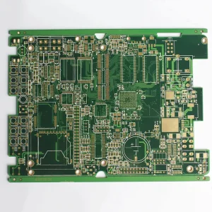
China High Density Interconnect (HDI) PCB from China - Leading Factory and Suppliers for Advanced Solutions Manufacturer, Factory
Configure Product
Engineered for extreme dynamic flexing, high-layer-count density, and robust thermal management in mission-critical environments.
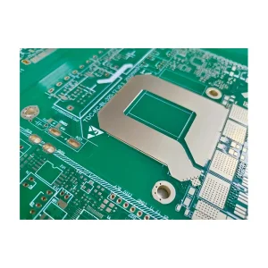
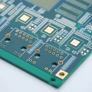
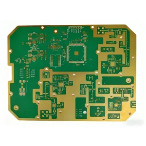
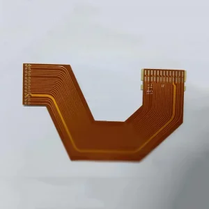
Modern electronic packaging demands dynamic flexural fatigue resistance, three-dimensional geometric conformability, and high-speed electrical integrity that legacy rigid FR-4 substrates can no longer sustain alone.
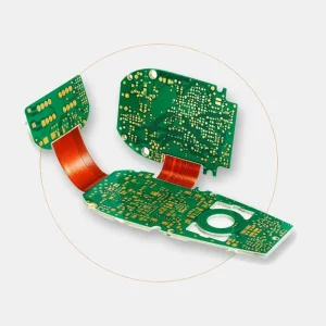
As smart systems, medical diagnostic implants, and airborne UAV payloads scale down in volume, volumetric space savings of up to 65% are attained by replacing bulky wire harnesses and heavy connectors with multi-layer polyimide flex circuits.
High-end Pc Board Flex fabrications undergo rigorous bending cycles exceeding 200,000 to 1,000,000 flexures without micro-cracking or copper trace work hardening, using adhesiveless electro-deposited (ED) or rolled annealed (RA) copper foils.
Polyimide cores exhibit superior glass transition points (TG > 260°C to 300°C) and continuous working temperatures from -200°C to +300°C, isolating high-heat components from catastrophic delamination in localized power converter hubs.
A granular engineering matrix covering micro-via formation, layer-stack allowances, and electro-chemical surface deposition.
| Engineering Parameter | Standard Flex Range | Advanced Rigid-Flex / HDI Capability | Process Validation Standards |
|---|---|---|---|
| Layer Count Capability | 1 to 6 Layers Pure Flex | 4 to 22 Layers Rigid-Flex (Stacked Vias) | IPC-6013 Class 2 & Class 3 |
| Core Substrate & Coverlay | 12.5µm – 50µm Polyimide (PI) / PET | Adhesiveless Polyimide + Modified Epoxies | IPC-4204 / IPC-4203 |
| Conductor Line / Space (Min) | 2.0 mil / 2.0 mil (50µm / 50µm) | 1.2 mil / 1.2 mil (30µm / 30µm via MSAP) | Automated Optical Inspection (AOI) |
| Laser Micro-Via Diameter | 0.10 mm (4 mil) UV Laser Drill | 0.05 mm (2 mil) Picosecond Laser Trepanning | Micro-section Cross-Check (MES) |
| Surface Finishes Available | ENIG (Electroless Ni / Immersion Au) | ENEPIG, Hard Gold (30-50µin), Immersion Tin | IPC-4552 / IPC-4556 |
| Stiffener Reinforcements | PI, FR-4 (0.1mm - 2.0mm) | Stainless Steel (SUS), Anodized Al, Copper Alloy | Optical Micro-alignment + CMM |
Bridging Shenzhen’s massive supply-chain ecosystem with Western procurement regulations and real-time localized engineering governance.
For high-reliability defense, aerospace, and medical implants, production undergoes rigid solder fillet cross-sectioning, automated 3D X-ray inspection (AXI) for BGA voiding under 10%, and ion chromatography ionic contamination tests.
Every polyimide roll, solder alloy batch, and surface-protection gold bath is 100% compliant with EU RoHS 3 and REACH regulations. We implement strict digital non-disclosure protocols and IP data security to prevent leakages across overseas customer designs.
Direct communication with certified PCB fabrication and assembly engineers in Shenzhen. Every quote is preceded by an in-depth Design for Manufacturability (DFM) review to identify impedance mismatches, stress points, and bend radius violations.
Real-world integration scenarios where rigid PCBs fail and specialized flexible interconnects dominate.
Multi-gigahertz microwave modules and RF phased-array antennas leverage low-loss Taconic/Rogers hybrid flex-rigid laminates. These boards withstand heavy gravitational G-forces and temperature fluctuations without mechanical fracture.
Replacing bulky copper cable harnesses, ultra-long flexible printed circuits (up to 1200mm) streamline battery cell voltage and thermistor telemetry directly to the ECU, cutting vehicle pack weight and assembly cycle times.
Sub-millimeter biocompatible flex circuits embedded in endoscopic probes, hearing implants, and dynamic continuous glucose monitors (CGM), populated with micro-pitch 01005 passives and lead-free micro-BGAs.
Continuous dynamic motion linkages in multi-axis robotic joints requiring billions of cyclic flexures. We employ custom rolled-annealed foil with specialized polyurethane outer-jackets to ensure non-stop manufacturing uptime.
Iterating next-generation manufacturing capabilities to support high-speed silicon co-packaging, photonic flex interfaces, and sustainable materials.
Full deployment of Semi-Additive Processes (mSAP) across flexible substrates to achieve 25µm line/space dimensions for advanced AI silicon chiplet carriers.
Hybrid electro-optical flex boards integrating polymer optical waveguides within standard polyimide stacks to bypass copper attenuation at 112Gbps PAM4 speeds.
Comprehensive transition to modified LCP dielectric substrates offering ultra-low moisture absorption (<0.04%) and exceptional Dk/Df stability past 100 GHz radar domains.
Eco-friendly, recyclable soluble organic polymers for disposable medical IoT electronics, reducing post-consumer e-waste footprint to zero.
In-depth responses curated by our manufacturing operations and DFM engineering teams.
Comprehensive electronic contract manufacturing solutions from prototype validation to high-volume multilayer production.