
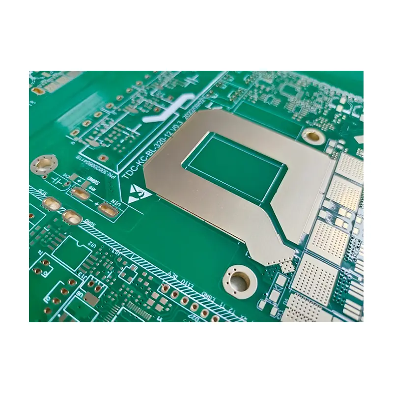
China High-Performance Heavy Copper PCB from China Suppliers | Factory Direct Power Converters for Optimal Heat Dissipation Manufacturer, Factory
Product Description
What is Heavy Copper PCB?
Core Features & Application Scenarios
Key Design Points
| Copper Thickness | Specification | Recommended Scenario |
|---|---|---|
| 70μm | 2 oz | Large current ≥ 5A circuits |
| 105μm | 3 oz | Medium-high power applications |
| 140μm | 4 oz | High-power industrial applications |
| 420μm | 12 oz | Ultra-power scenarios ≥ 20A |
Current-Carrying Capacity Calculation:
- Must combine copper thickness, line width, and temperature rise requirements (typically designed for a 10℃ temperature rise).
- Formula: I = K × W × T0.83 (I = current, K = coefficient, W = line width, T = copper thickness)
- Example: 2 oz copper (70μm), wire width 5mm → current-carrying capacity ≈ 15A (at 10℃ temperature rise)
- Vias: For high-current vias, increase hole diameter (≥ 0.5mm), increase the number of vias (estimated at 1A per hole), and ensure copper plating thickness on hole wall ≥ 20μm (vs. 8–12μm for standard PCBs).
- Pads: Thick copper pads must be enlarged (0.2–0.5mm larger than standard pads) to prevent the copper layer from dissipating heat too quickly during soldering, which may cause false soldering.
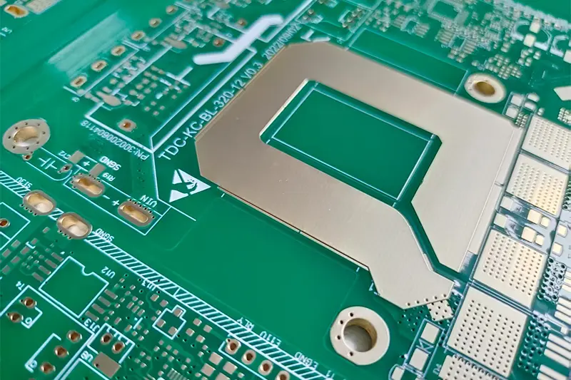
- Heat Dissipation: The thick copper area can be designed as a "copper sheet heat sink," or a metallized via array (via spacing ≤ 1mm) can be added to connect to the heat dissipation layer.
- Insulation: Wire spacing for thick copper layers must be widened (for 70μm copper, spacing ≥ 0.2mm) to prevent creepage breakdown under high voltage.
Manufacturing Process Difficulties & Control
Thick Copper Lamination: High-temperature and high-pressure lamination (180℃ / 4MPa) is required to ensure peel strength between copper foil and substrate (≥ 1.2N/mm).
Thick Copper Etching: The etching rate is slow (approx. 1μm/min). Etching time must be carefully controlled to avoid side etching (side etching amount ≤ 0.05mm). A stepwise etching process should be adopted to reduce line width deviation.
The coefficient of thermal expansion (CTE) of thick copper layers differs significantly from that of the substrate. When laminating, a "symmetrical structure" (consistent copper thickness between upper and lower layers) should be adopted, and a rigid support layer should be added to prevent PCB warping (warping degree ≤ 0.5%).
The surface of thick copper is prone to oxidation. It is preferred to choose tin plating (high-temperature tin layer) or nickel-gold plating to avoid OSP (incomplete organic film coverage).
The pad area needs to be enlarged with a "solder mask opening window" to ensure the bonding force between the solder and thick copper.
Core Summary
The core of heavy copper PCBs is "high current-carrying capacity + superior heat dissipation." In terms of design, it is essential to match the copper thickness with current-carrying capacity requirements. In manufacturing, challenges such as thick copper etching and lamination warping must be resolved. Heavy copper PCBs are ideally suited for high-power, high-current industrial and energy applications.









