
Featured Industrial PCB Circuit Configurations
Explore our top-tier circuit substrate solutions engineered for heavy thermal dissipation, microwave radar transceivers, IoT micro-modules, and dynamic rigid-flex architectures.

OEM High Thermal Conductivity Aluminum PCB from China - Leading Suppliers & Factory for Efficient Circuit Solutions Manufacturer, Suppliers
View Specifications & Pricing
Famous China Raspberry Pi HAT - Quality Expansion Boards from Trusted Suppliers and Factory for DIY Projects Manufacturer, Factory
View Specifications & Pricing
ODM High-Quality RF & Microwave PCBs from China Suppliers and Factory for Mobile Phones & Radar Systems, ≥500MHz Frequency Manufacturers, Supplier
View Specifications & Pricing
ODM China Raspberry Pi HAT: Top Suppliers and Factory Innovations for Mini Single-Board Computer Projects Quotes, Factories
View Specifications & Pricing
Buy China Rigid Flex PCB Suppliers - Single & Double-Sided, 4-16 Layer Multi-Layer Flex PCB Factory Supplier, Company
View Specifications & Pricing
ODM High Frequency PCB Solutions: Minimize Signal Loss, Crosstalk, and EMI from China Suppliers and Factory Quotes, Pricelist
View Specifications & Pricing
Famous Heavy Copper PCB from China Suppliers - Durable, High-Performance Components for Power Converters and Vehicles Supplier, Companies
View Specifications & Pricing
Buy High-Quality Heavy Copper PCBs from China Factory: Ideal for Power Converters and Strong Current Applications – Top Suppliers Company, Factory
View Specifications & PricingNavigating Enterprise PCB Sourcing: Resilience & TCO Analysis
Modern hardware brands face complex geopolitical barriers, volatile component allocations, and stringent time-to-market demands. PCB ADEPT (Shenzhen ICSLOVE Technology Co., Ltd.) restructures your electronics supply chain with transparent direct-factory governance.
Single-Point Accountability
Overseas procurement teams often suffer from disjointed vendor chains—board fabrication in one shop, component brokers in another, and manual assembly lines elsewhere. PCB ADEPT integrates bare board fabrication, authorized component kitting, SMT/DIP placement, and box build under one roof in Bao'an, Shenzhen, eliminating finger-pointing.
Direct BOM Optimization
With an active component sourcing team bringing over a decade of distribution partnerships with Texas Instruments, Analog Devices, STMicroelectronics, Microchip, Murata, and TE Connectivity (Tyco), we offer pin-to-pin drop-in alternatives for hard-to-find chips, cutting BOM costs by up to 15% without sacrificing reliability.
Rapid NPI-to-Volume Bridge
Our rapid prototyping facility runs 1 to 500 pcs quick-turn assemblies within 3 to 9 days. Once engineering validation completes, products transition seamlessly to our 6 automated SMT lines and 4 wave-soldering DIP lines, ensuring unified thermal profiles, stencils, and MES testing programs without requalification delays.
Macro-Industry Electronic Manufacturing Solutions
Every sector presents unique dielectric losses, vibrational stresses, thermal thresholds, and compliance mandates. Our Shenzhen facility custom-calibrates manufacturing process windows for mission-critical deployments.

RF & Telecommunications
High-frequency microwave boards using Rogers 4003C/4350B and Taconic PTFE laminates. Tight Dk control (±0.05) and phase-matched line tolerances for 5G base stations, phased arrays, and satellite transceivers.

Defense & Anti-Drone Systems
Solid aluminum-backed power boards and hybrid FR-4/PTFE stacks designed for multi-band signal disruption, drone radar detection, high-power GaN amplifier modules, and directional RF antennas.

Aerospace & Avionics
IPC Class 3 manufacturing with hard gold plating, ENEPIG finishes, vacuum de-aeration, and blind/buried microvias capable of surviving extreme G-forces, thermal cycling (-55°C to +125°C), and altitude shock.

Smart Consumer Electronics
High-density interconnect (HDI) boards supporting ultra-compact 01005 passives and 0.35mm pitch BGAs for audio wearables, handheld controllers, gaming peripherals, and domestic automation gateways.

Energy & E-Mobility
Heavy copper PCB circuitry (up to 10oz) combined with thermally conductive prepregs. Engineered for EV traction inverters, high-voltage battery management systems (BMS), solar micro-inverters, and DC charging piles.

Industrial Control & Robotics
Robust 4 to 22-layer rigid-flex boards designed for continuous articulation inside robotic joints, PLC modules, servo motor drives, and legacy industrial controller reverse-engineering replication.

IoT & Wireless Sensing
Low-power, battery-optimized flex and rigid architectures featuring integrated BLE, LoRa, Wi-Fi 6, and Zigbee antennas with conformal coating for outdoor smart metering and asset-tracking telematics.

Medical Devices & Diagnostics
Biocompatible flexible circuits and multi-layer rigid boards for diagnostic imaging, vital sign monitors, and portable infusion pumps, backed by full component traceability and ISO 13485 cleanroom protocols.
Engineering Capabilities & Fabrication Tolerance Matrix
Review our process engineering parameters before uploading your Gerber (RS-274X, ODB++) and IPC-2581 files. We support everything from rapid double-sided prototypes to 60-layer multi-tier HDI boards.
| Manufacturing Parameter | Standard Capability | Advanced / Cutting-Edge | Industry Compliance |
|---|---|---|---|
| Layer Count Range | 1 – 8 Layers (FR-4 / CEM-1) | 10 – 60 Layers (Multi-Tier Any-Layer) | IPC-6012 Class 2 / 3 |
| Min. Trace Width / Spacing | 3.5 mil / 3.5 mil (0.089mm) | 2.5 mil / 2.5 mil (0.063mm - mSAP) | High-Density HDI |
| Microvia / Mechanical Hole | Laser: 0.10mm | Mech: 0.15mm | Laser: 0.075mm | Mech: 0.10mm | VIPPO Plug & Plate |
| Base Copper Thickness | 0.5 oz – 2 oz (18μm – 70μm) | 3 oz – 10 oz Heavy Copper Power | UL 94V-0 |
| Controlled Impedance | ±10% Standard Single/Diff | ±5% High-Precision TDR Verified | Polar SI8000 |
| Core Substrate Formats | Shengyi S1000-2M, ITEQ, Kingboard | Rogers 4350B/3003, Taconic, Megtron 6 | RoHS & REACH |
| Surface Finishes | HASL Lead-Free, OSP, ENIG (1-3u") | ENEPIG, Hard Gold (30u"), Immersion Ag | IPC-4552 / IPC-4556 |
| SMT Component Placement | 0402, 0603, 0805, QFP, SOIC | 01005, 0201 Passives, 0.35mm Pitch BGA | IPC-A-610 Class 3 |
Substrate-Like PCB (SLP) Evolution
As microelectronics shrink, PCB ADEPT incorporates Modified Semi-Additive Processes (mSAP). This yields ultra-sharp conductor profiles with vertical sidewalls, allowing high-speed DDR5 and PCIe 5.0 lines to maintain pristine signal integrity across tight geometries.
Embedded Passives & Cavity PCBs
To support high-frequency RF modules and anti-drone electronics, we fabricate internal cavity PCBs with embedded copper coins and passives buried within prepregs, delivering supreme electromagnetic shielding and shortened heat paths.
Thermally Dissipative Substrates
From single-layer insulated metal substrates (IMS) with 3.0 W/mK to direct copper bonding (DCB) ceramic carriers, we design custom thermal conduction planes for kilowatt-tier solar converters and automotive power electronics.
PCB Fabrication & Assembly Pricelist Guide (2025–2026)
Eliminate commercial broker markups. Our open-book cost breakdown highlights baseline prices for quick-turn prototypes and medium-volume series, helping engineering heads optimize BOM budgets.
| Substrate Technology | Layer Count | Prototype (1–10 pcs) | Batch (100–500 pcs) | Mass Volume (>1,000 pcs) | Standard Lead Time |
|---|---|---|---|---|---|
| Standard FR-4 (TG140) | 2 Layers | $25 – $45 total | $1.20 – $2.50 / board | $0.45 – $0.95 / board | 3 – 4 Days (Fast-turn 24h) |
| Multilayer FR-4 (TG170) | 4 Layers | $55 – $85 total | $2.80 – $4.90 / board | $1.40 – $2.20 / board | 4 – 5 Days (Fast-turn 48h) |
| High-Layer Precision | 6 – 8 Layers | $110 – $195 total | $5.50 – $9.20 / board | $3.20 – $5.80 / board | 6 – 8 Days |
| Any-Layer HDI (1+N+1) | 4 – 10 Layers | $220 – $380 total | $9.80 – $16.50 / board | $6.20 – $10.50 / board | 8 – 12 Days |
| Aluminum Metal Core (1-3 W/mK) | 1 – 2 Layers | $40 – $75 total | $1.90 – $3.80 / board | $0.95 – $1.80 / board | 3 – 5 Days |
| Heavy Copper (3oz – 6oz) | 2 – 6 Layers | $140 – $260 total | $7.20 – $13.50 / board | $4.80 – $8.90 / board | 7 – 9 Days |
| Flex & Rigid-Flex PCB | 4 – 8 Layers | $180 – $340 total | $8.50 – $15.20 / board | $5.60 – $10.10 / board | 9 – 14 Days |
| High Frequency (Rogers 4350B) | 2 – 4 Layers | $160 – $290 total | $8.90 – $17.50 / board | $6.50 – $12.80 / board | 7 – 10 Days |
Turnkey SMT Setup Models
Stencil Fee: $15 – $30 (Laser Stainless).
SMT Setup per Line: $30 – $60 (Waived on volume >500 pcs).
SMT Point Rate: $0.003 – $0.006 per soldering point.
BGA / Fine Pitch X-Ray: Free with every prototype run.
Surface Finish Surcharges
HASL Lead-Free: Included as standard.
ENIG (Electroless Nickel Immersion Gold): +$15–$35 per panel lot.
ENEPIG (Wire-Bondable Gold): Cost based on gold index.
Immersion Silver / Tin: Low-loss planar finishes on demand.
BOM Sourcing Guarantee
Transparency: Sourced directly via franchise channels.
Traceability: CoC (Certificate of Conformance) provided.
Warehousing: Common SMD passives free from our stock.
Payment Terms: Net terms available for qualified accounts.
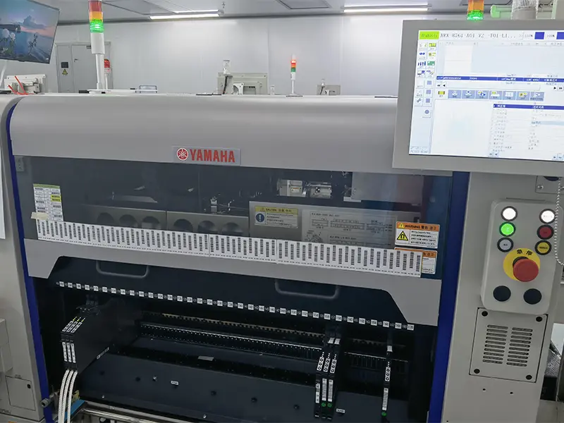
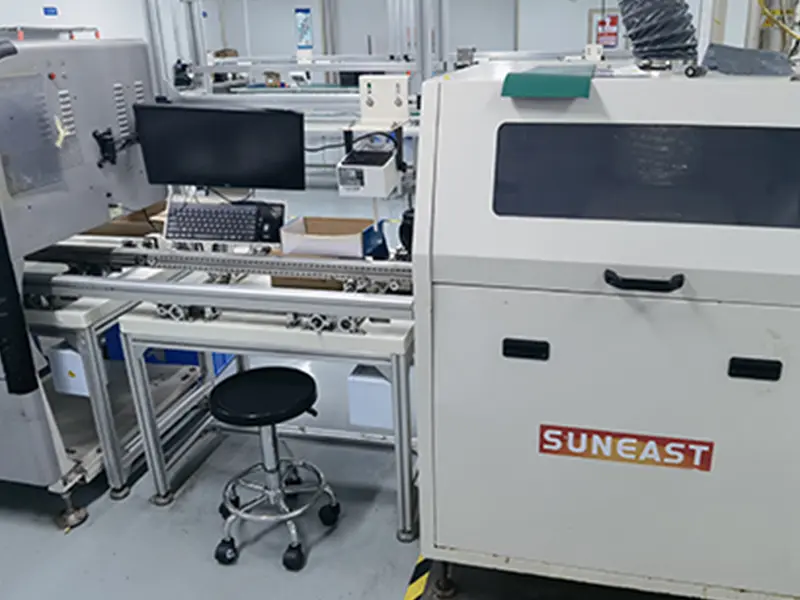
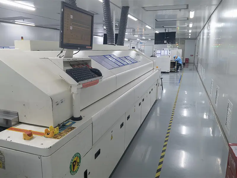
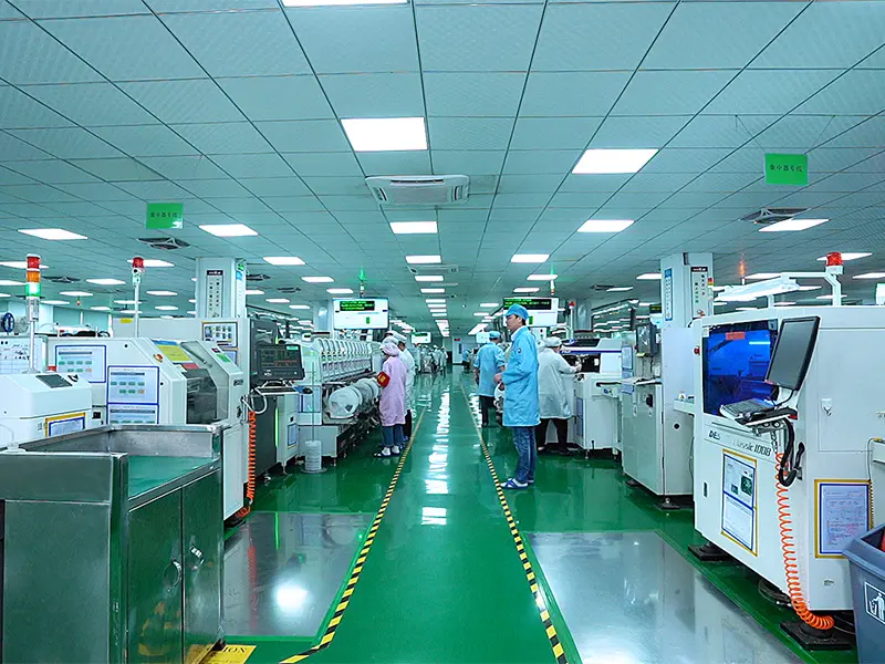
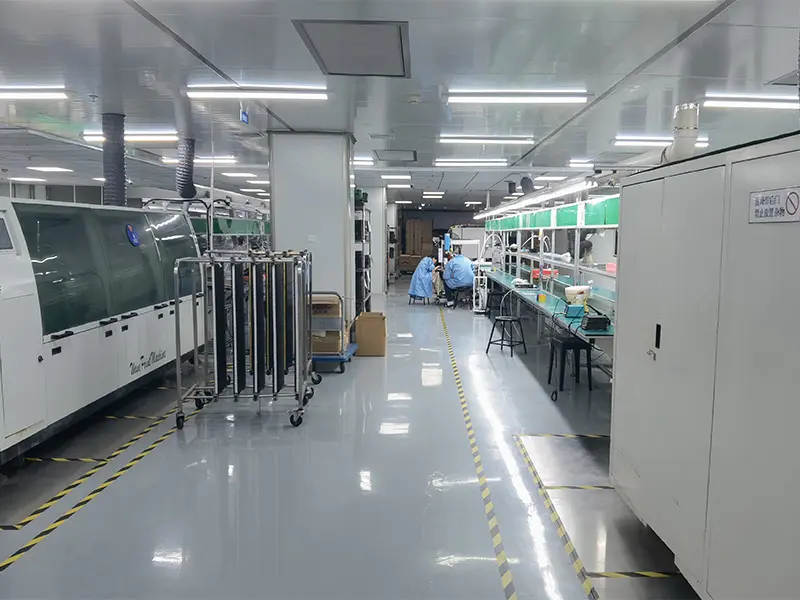
Shenzhen Bao'an Hub: Inside Our 8,000 m² Facility
Located in the heart of China's electronics capital—Anda Electronic Industrial Zone, Fuhai Subdistrict, Bao'an District, Shenzhen—our workshop operates under complete MES digital control with 6 automated SMT lines and 4 DIP lines.


Audited Quality Management & Enterprise Endorsements
Every PCB batch ships with full QA documentation: IPC-A-600/610 inspection certificates, micro-section analysis, solderability reports, and RoHS/REACH compliance declarations.
ISO 9001:2015
Certified Quality System covering entire SMT, DIP, fabrication, and sourcing workflows with full MES data logging.
UL 94V-0 Recognized
Tested flammability compliance with official yellow-card traceability for high-voltage and industrial power electronics.
RoHS 3 & REACH
Strict lead-free assembly processes. Regular testing guarantees zero restricted heavy metals or toxic halogens.
IPC Class 2 & 3
Certified assembly and inspection criteria according to IPC-A-610 Class 3 for mission-critical aerospace and medical boards.
Trusted by Hardware Innovators & Electronics Brands










Rapid Prototyping & Modular Expansion Series
Accelerate your pilot builds with 48-hour multilayer fabrication and custom expansion HAT platforms tailored for embedded IoT developers and industrial OEMs.

High-Quality China PCB Factory: Top Suppliers for Rapid Prototyping and Validation in Electronics Development Suppliers, Pricelist
View Specifications & Pricing
China China Raspberry Pi HAT - High-Quality Expansion Boards from Trusted Suppliers and Factory Quotes, Factories
View Specifications & Pricing
Buy China Suppliers and Factory for Raspberry Pi HAT: Enhance Your Projects with Versatile Expansion Boards Supplier, Companies
View Specifications & Pricing
ODM Rapid PCB Prototyping and Validation Solutions: Top China Suppliers and Factory for Modern Electronics Quotes, Pricelist
View Specifications & Pricing
Famous Raspberry Pi HAT from China Factory: Top Suppliers for Mini Single-Board Computer and IoT Projects Pricelist, Factory
View Specifications & Pricing
High-Quality High-Quality Aluminum PCB from China Factory - Leading Suppliers for Thermal Management Solutions Pricelist, Factories
View Specifications & Pricing
High-Quality High-Quality 1-60 Layers Multilayer PCB from China Supplier - Fastest Lead Time 48 Hours, IPC2 Grade Factory Manufacturers, Manufacturer
View Specifications & Pricing
High-Quality China PCB Prototyping and Validation: Leading Suppliers and Factory Solutions for Rapid Product Development Supplier, Companies
View Specifications & PricingEngineering Whitepapers & Manufacturing Insights
Read in-depth technical guides authored by our chief electronics engineers covering flexible PCB vetting, surface mount technology optimization, and supply chain management.

Top 5 Qualities to Look for in a Reliable OEM Flexible PCB Board Manufacturer in 2026
How hardware architects vet flex PCB suppliers on raw polyimide quality, dynamic bend radius life, laser micro-etching tolerances, and MES lot traceability.
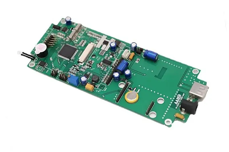
What Is PCBA? The Comprehensive Assembly Process Explained
From solder paste rheology and 3D SPI volume checks to high-speed placement, 10-zone reflow profiles, and automated flying probe functional validation.
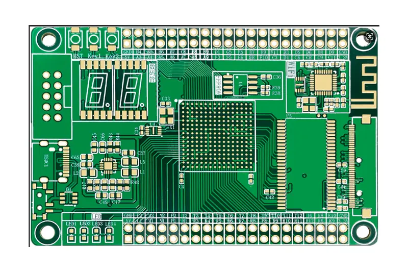
What Is a PCB? Substrate Layers, Copper Physics & Dielectrics
Deconstructing bare board laminates, prepregs, woven glass styles, thermal expansion coefficients (CTE), and copper foil surface roughness for signal integrity.

Shenzhen ICSLOVE Technology Relocates to Anda Industrial Zone
Expanding to 8,000 m² cleanroom manufacturing capacity in Bao'an District, Shenzhen, adding 2 new automated high-speed Yamaha SMT lines and 3D AOI stations.
Frequently Asked Questions: PCB Fabrication, Assembly & Sourcing
Clear, technically accurate answers to the questions hardware engineering leads and procurement directors ask before issuing requests for quotes (RFQs).
What is the minimum order quantity (MOQ) and lead time for PCB assembly?
For prototype engineering validation and trial-run pilot batches, our MOQ is strictly 1 piece, scaling up to 500 pieces. Quick-turn PCBA lead time is typically 3 to 9 business days, provided component procurement is expedited. Fast-track bare board fabrication can be delivered within 24 to 48 hours for urgent R&D milestones.
Which exact file packages are required to generate an instant, accurate quote?
We request standard Gerber RS-274X or ODB++ fabrication data, an engineering bill of materials (BOM) in Excel with clear Manufacturer Part Numbers (MPN) and authorized distributors, a centroid pick-and-place (.xy or .txt) coordinate file, and an assembly drawing. If MCU firmware flashing or functional testing (FCT) is requested, please include programming and test scripts.
How does PCB ADEPT guarantee 100% component authenticity and avoid grey-market counterfeits?
Our centralized sourcing department brings 10+ years of procurement experience with direct franchise relationships: DigiKey, Mouser, Arrow, Avnet, and official domestic Tier-1 brand distributors. We source strictly factory-original packaging with verifiable lot codes and Certificates of Conformance (CoC). Every shipment undergoes IQC X-ray and solderability sampling before entering cleanroom stock.
What testing procedures are included in standard turnkey PCB assembly?
Our baseline quality control includes Solder Paste Inspection (SPI), First Article Inspection (FAI) using automated LCR comparators, inline pre-reflow and post-reflow 3D Automated Optical Inspection (AOI), X-ray inspection for all BGA, QFN, and leadless power pads, and electrical flying probe or bed-of-nails E-testing for bare boards. Custom FCT, burn-in aging, and thermal chamber tests are available on demand.
Can PCB ADEPT handle complex hybrid RF, heavy copper, and rigid-flex stack-ups?
Yes. Our engineering division specializes in hybrid press-bonding (e.g., Rogers 4350B high-frequency PTFE layers bonded onto FR-4 backplanes), heavy copper up to 10oz for industrial motor controllers, and 4 to 22-layer dynamic rigid-flex circuits with adhesiveless polyimide and selective FR-4/aluminum stiffeners, engineered to withstand over 100,000 continuous flex cycles.
Do you support box build electromechanical assembly and finished goods fulfillment?
Beyond PCBA, our Bao'an facility provides full box-build electromechanical integration. We handle plastic injection molding, high-precision CNC metal enclosure milling, silicone sealing, wire-harness routing, potting, display integration, functional device testing, laser engraving, packaging, and direct DDP shipping to your distribution hubs in Europe, the Americas, and APAC.
How does DFM review work, and how quickly do I receive engineering queries?
Within 2 hours of file upload, our dedicated CAM and DFM engineers run automated design rule checks (DRC) to detect trace-to-pad clearances, acute acid-trap angles, missing thermal reliefs, mismatched footprints, and solder-mask bridging. We return a clean DFM report with recommended stack-ups and panelization drawings for customer approval prior to tooling.
What international logistics channels and import payment terms do you support?
We work with DHL, FedEx, and UPS priority air freight (typically 3 to 5 business days delivery worldwide) alongside sea and air consolidation for palletized volume orders. We offer DAP and DDP shipping terms, handling all customs clearance and tariffs directly. Payment options include wire transfer (T/T), PayPal for prototypes, and flexible credit terms (Net 30/60) for long-term contract partners.
Initiate Your Next High-Reliability PCB Circuit Build
Upload your Gerber files and BOM today. Our Shenzhen engineering team will provide a comprehensive DFM audit, detailed impedance stack-up verification, and a transparent price quotation within 2 hours.