High-Quality China PCB Factory: Top Suppliers for Rapid Prototyping and Validation in Electronics Development Suppliers, Pricelist

,

PCB (Printed Circuit Board) technology lies at the heart of the modern electronics and technology industries. The quality of a circuit board significantly influences the performance of electronic products, which is closely tied to the expertise of R&D designers as well as the manufacturing capabilities and management standards of PCB suppliers in China.

,

Speed to Market: Why Rapid PCB Prototyping and Validation are Essential for Success**

,

In today's fiercely competitive electronics market, the principle fast eats the slow underscores the importance of quick product launches. A product's time-to-market is often the determining factor for its success. Within this dynamic environment, **rapid PCB (Printed Circuit Board) prototyping and thorough product validation** serve as vital links between innovative design and mass production, establishing them as critical components of the product development process in factories across China.

,

Product Description

A Historical Perspective: The Evolution from "Months" to "Days"

Looking back at the history of the electronics industry, PCB manufacturing was once a lengthy and painful bottleneck.

  • ▶
    The Manual Era (Mid-20th Century): In the early days, circuits were built using "point-to-point" wiring, which was bulky and unreliable. The advent of PCBs was a major step forward, but the process relied entirely on manual drafting, film exposure, and chemical etching. An iteration cycle could take weeks or even months.
  • ▶
    Standardization and the CAM Era (Late 20th Century): With the development of Computer-Aided Manufacturing (CAM) technology, the Gerber format became the standard, enabling the initial digital separation of design and manufacturing. However, the process still required physical film and tooling (e.g., drilling NC programs), remaining cumbersome.
  • ▶
    The Rapid Prototyping Revolution (Early 21st Century – Present): The internet, Laser Direct Imaging (LDI), automated precision drilling, and standardized materials gave rise to specialized quick-turn PCB services. Through online ordering, automated production lines, and efficient logistics networks, they have compressed PCB prototype lead times from "weeks" to "days," fundamentally changing the game.
※
The Historical Lesson: Each technological advancement has compressed the time from "idea" to "physical object." This increase in speed has essentially transformed product development from a serial, high-cost "gamble" into a parallel, low-cost process of "rapid iteration and failure."
Rapid Prototyping and Product Validation: The Flywheel for Accelerated Market Launch

The value of rapid prototyping lies not just in its speed, but in how it empowers the entire validation process.

①
Functional Validation

This is the core step. After assembling the board, engineers perform power-on tests and basic debugging to verify the circuit design is correct. Rapid prototyping allows design teams to discover and fix schematic or component selection errors within days.

②
Performance Validation

In high-frequency, high-speed, or high-power applications, PCB layout is critical to signal integrity, power integrity, and Electromagnetic Compatibility (EMC). Prototypes enable early lab testing to assess whether strict performance metrics are met.

③
DFM/DFA Validation

This is Design for Manufacturability/Assembly validation. The physical board allows engineers to check component placement, spacing, thermal management, and suitability for automated assembly. Identifying DFM/DFA issues early prevents massive losses during mass production.

④
Mechanical and Form Factor Validation

Prototypes help verify that the PCB's dimensions, shape, and connector positions perfectly match the product enclosure, providing accurate data for mechanical design.

⚡
The Logic of Speed: Each rapid "design-prototype-validate" iteration eliminates a potential risk point. The shorter the iteration cycle, the more validation rounds can be completed in a given time, accelerating the product's maturity and ensuring a smooth transition to mass production and a high-quality market launch.
Technological Advancements: The Foundation of Rapid Manufacturing

Modern rapid prototyping is enabled by several key technologies:

Laser Direct Imaging LDI

Laser Direct Imaging (LDI)

Replaces physical film by using a laser to image the photoresist directly, offering high precision, speed, and adaptability for small-batch, high-mix production.

Automation and Digital Workflows

Automation and Digital Workflows

From Automated Optical Inspection (AOI) to flying probe testing and automated material handling, these processes minimize manual intervention, increasing efficiency and consistency.

High-Performance Materials

High-Performance Materials

A wide range of materials, from standard FR-4 to high-frequency/low-loss (e.g., Rogers), high-Tg, and flexible substrates (PI), meets the rapid needs of diverse applications.

Online Collaboration Platforms

Online Collaboration Platforms

Customers submit Gerber files online, and the system automatically performs DFM analysis and provides instant quotes, streamlining the ordering process.

Common PCB Types and Key Process Parameter Requirements

Modern rapid prototyping is enabled by several key technologies:

Image PCB Type Description Key Process Parameters
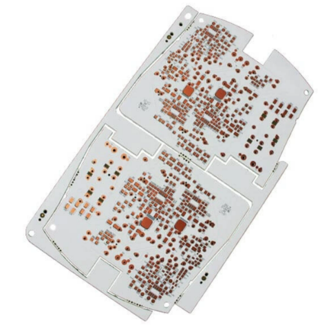
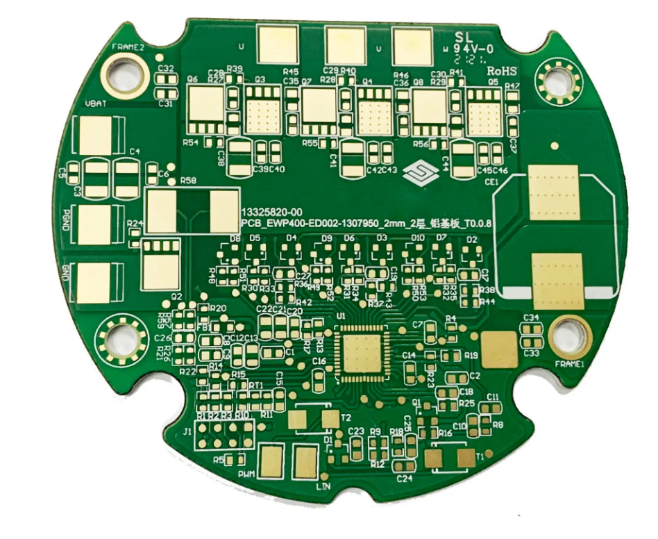
Single-Sided PCB Single-Sided Lowest cost, simple structure. Used in low-density consumer electronics. Board Thickness: 1.0mm, 1.6mm
Copper Weight: 1oz (35μm)
Min. Trace/Space: 0.2mm
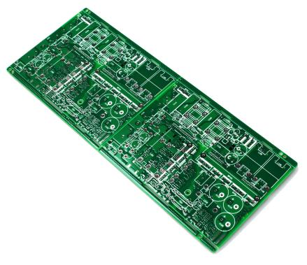
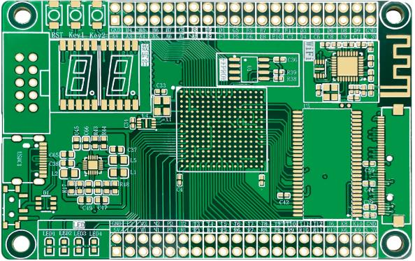
Double-Sided PCB Double-Sided The most common type, routing on both sides. Used in most standard electronic products. Board Thickness: 1.0mm, 1.6mm
Copper Weight: 1oz / 1oz
Min. Trace/Space: 0.15mm / 0.1mm
Vias: Mechanically drilled, hole size ≥0.3mm
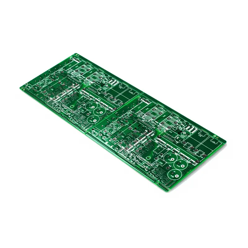
Multi-Layer PCB Multi-Layer High density, high performance. Used in complex circuits like smartphones, industrial controls, and communication equipment. Layers: 4–12 (common)
Board Thickness: 1.0mm, 1.6mm
Inner Layer Copper: 0.5oz / 1oz
Min. Trace/Space: 0.1mm / 0.1mm
Blind/Buried Vias: Increases cost, must be specified
High-Frequency High-Speed PCB High-Freq./High-Speed Low loss, stable Dk/Df. Used in 5G, radar, satellite communication. Material: Rogers, Taconic, etc.
Loss Tangent (Df): Must be very low (e.g., Df < 0.004)
Surface Finish: Often ENIG (Immersion Gold) for signal quality
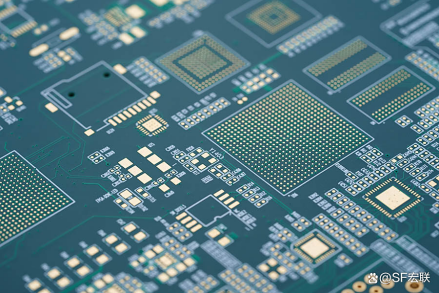
HDI PCB HDI High-Density Interconnect, uses micro-vias. For space-constrained portable devices. Min. Trace/Space: ≤0.075mm
Laser Drilled Via Size: 0.1mm or smaller
Stacked Via Structures: Any-layer interconnects
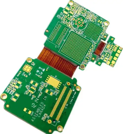
Flex Rigid-Flex PCB Flex/Rigid-Flex Bendable, 3D assembly. Used in cameras, medical devices, wearables. Substrate: Polyimide (PI)
Bend Radius: A critical parameter
Lamination Process: Complex for rigid-flex zones
Conclusion
🏁
Rapid PCB prototyping has evolved from a supporting service into a strategic pillar of modern electronics innovation. It deeply embodies the modern R&D philosophy that "time is market, and validation is value." By understanding its critical importance, learning from historical trends and technological advancements, and mastering the process requirements for different PCB types, companies can build an efficient and reliable "design-validate-iterate" loop. This enables them to seize the initiative in a fiercely competitive market and ultimately win the race to bring successful products to market.
Send Inquiry

Your Name*

E-mail*

Phone Number

Country

Remarks*

reset
Frequently Asked Questions (FAQ)
Q
What is rapid PCB prototyping and why is it important for product development?
Rapid PCB prototyping is the process of quickly manufacturing a small number of printed circuit boards from design files to validate a concept before mass production. It is critically important because it compresses the "design-validate-iterate" cycle from weeks to days, allowing engineering teams to identify and correct design flaws early — dramatically reducing the risk and cost of errors discovered during mass production.
Q
How fast can a rapid PCB prototype be delivered, and what factors affect lead time?
Modern rapid PCB services can deliver standard prototypes in as little as 24–72 hours for simple single- or double-sided boards. Lead time is affected by several factors including the number of layers, complexity of features (e.g., blind/buried vias, HDI structures), selected material (standard FR-4 vs. Rogers high-frequency), surface finish, and the quantity ordered. Providing complete and correct Gerber files also helps avoid delays from DFM review corrections.
Q
What types of PCBs can be produced through rapid prototyping services?
Rapid prototyping services support a wide range of PCB types, including single-sided, double-sided, multi-layer (typically 4–12 layers), high-frequency/high-speed boards using materials like Rogers or Taconic, HDI boards with laser-drilled micro-vias, and flexible or rigid-flex boards on polyimide substrates. Each type has different process requirements, and it is important to communicate your specific parameters when placing an order.
Q
What files do I need to submit for a PCB prototype order, and how does the online process work?
The standard requirement is a complete Gerber file set (RS-274X format), which includes all copper layers, solder mask layers, silkscreen layers, board outline, and drill files (Excellon format). Most modern online platforms also accept native EDA formats. Once uploaded, the system automatically performs a DFM (Design for Manufacturability) check and generates an instant quote. You then confirm specifications such as layer count, board thickness, copper weight, surface finish, and solder mask color before placing the order.
Q
What is DFM validation, and why should it be done at the prototype stage?
DFM stands for Design for Manufacturability. It is the process of evaluating a PCB design to ensure it can be reliably and cost-effectively manufactured at scale. Conducting DFM validation at the prototype stage — rather than after tooling and production ramp-up — allows engineers to identify and resolve issues such as insufficient trace spacing, improper pad sizes, thermal management problems, or assembly clearance conflicts before they become extremely expensive to fix. Early DFM review is one of the most cost-effective investments in a product development cycle.
Q
What is the difference between Laser Direct Imaging (LDI) and traditional film-based imaging in PCB manufacturing?
Traditional film-based imaging requires creating a physical photomask (film) for each PCB design, which takes time and is sensitive to environmental conditions such as temperature and humidity. Laser Direct Imaging (LDI), by contrast, uses a computer-controlled laser to expose the photoresist directly from digital data — eliminating the need for physical film entirely. LDI offers superior registration accuracy, faster setup, and is far more flexible for small-batch and high-mix production, making it a cornerstone technology for rapid PCB prototyping services.

Related Products