
ODM High Frequency PCB Solutions: Minimize Signal Loss, Crosstalk, and EMI from China Suppliers and Factory Quotes, Pricelist
Product Description
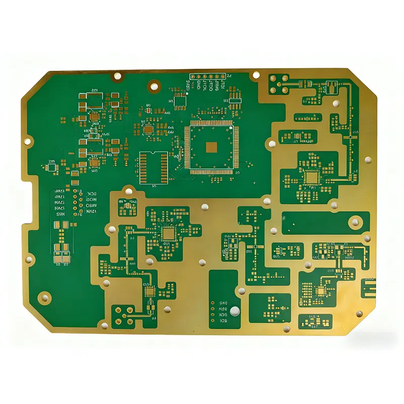
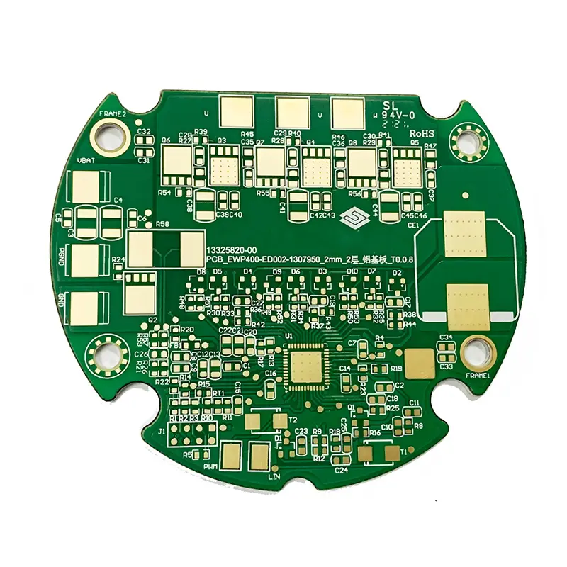
High-frequency PCBs are special printed circuit boards specifically designed to handle high-frequency signals (typically referring to frequencies above 500MHz or digital signal rise times less than 1 nanosecond).
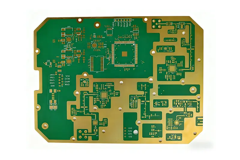
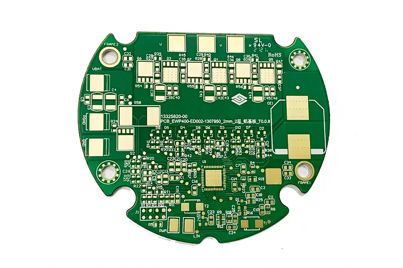
High-frequency signals are easily affected by the dielectric properties and losses of the substrate. Material selection is the core of high-frequency PCBs.
| Material Type | Key Parameters | Recommended Material / Specification | Applicable Scene |
|---|---|---|---|
| Base Material |
Dielectric constant (Dk) Dielectric loss tangent of angle (Df) Coefficient of thermal expansion (CTE) |
High-frequency dedicated substrate — PTFE (polytetrafluoroethylene, Dk=2.1–2.6, Df≤0.0009) — Rogers series (e.g. RO4350B, Dk=3.48, Df=0.0037) — Modified epoxy resin (FR-4 high-freq version, Dk=3.8–4.2, Df≤0.01) |
PTFE/Rogers: Millimeter wave, radar, 5G base station High-freq FR-4: Consumer electronics (mobile phones, routers) |
| Copper Foil | Surface roughness | Low profile copper foil (LP) / very low profile copper foil (VLP), roughness ≤1.0μm | Reduce the transmission loss of signals on the surface of copper foil (skin effect) |
| Solder Mask Layer | Dielectric loss | High-frequency special solder mask oil (Df≤0.01) | Avoid increasing signal attenuation by the solder mask layer |
- The core of high-frequency PCBs needs to control the characteristic impedance (e.g. 50Ω single-ended, 100Ω differential), with deviation ≤±5% (±10% for ordinary PCBs).
- Impedance calculation: Combine base material Dk, plate thickness, line width/spacing, and copper foil thickness. Simulate via professional software (e.g. Polar SI9000).
- Example: RO4350B substrate (thickness 0.254mm), single-ended 50Ω corresponds to approximately 0.8mm line width.
- Impedance compensation: Reserve ±0.02mm for line width considering etching side erosion and solder mask coverage.
- Traces should be as short and straight as possible; avoid right angles or acute angles (prone to reflection at high frequencies). Fillet radius should be no less than 0.5mm.
- Differential traces should be equal length and spacing (length difference ≤5mil), with ground wrapping (distance between ground wire and differential wire ≤2× line width) to reduce EMI.
- Skin effect response: High-frequency current concentrates on the copper foil surface. Silver-plated copper foil can be used to reduce surface resistance, or traces can be widened to reduce current density.
- Complete ground layer: High-frequency PCBs need a complete GND Plane — avoid ground layer segmentation. Distance between ground layer and signal layer should be no more than 0.2mm.
- Shielding measures: For sensitive RF areas (e.g. RF chips), metal shielding covers can be designed. Grounding must be reliable (multiple points, spacing ≤λ/20).
- Heat dissipation: High-frequency devices (e.g. power amplifiers) generate significant heat. Design heat dissipation pads and metallized via arrays (via diameter ≥0.3mm, spacing ≤1mm).
- Device packaging: Prioritize miniaturized, low-parasitic packaging (e.g. QFN, LGA) to reduce signal reflection.
- Line width/spacing tolerance: ≤±0.01mm (vs ±0.02mm for ordinary PCBs). Use high-precision Laser Direct Imaging (LDI) to replace traditional film exposure.
- Lamination accuracy: Interlayer alignment deviation ≤0.02mm. Bonding temperature and pressure must match base material characteristics (e.g. PTFE requires high-temperature, high-pressure bonding).
- Etching process: Micro-etching technology reduces copper foil surface roughness and avoids increased transmission loss. Lateral erosion ≤0.01mm.
- Surface treatment: Electroless nickel gold plating (ENIG) or silver plating is preferred over OSP (organic film increases contact resistance). Gold layer thickness should be ≤0.1μm — thicker layers increase loss.
The core of high-frequency PCBs lies in "reducing signal loss, ensuring precise impedance, and minimizing electromagnetic interference". It requires full-process control: from low-loss substrate selection → precise impedance design → high-precision manufacturing. For different high-frequency scenarios (e.g. 1GHz vs 60GHz), substrate and process parameters must be specifically adjusted.
High-frequency PCBs typically handle signals above 500MHz, or digital signals with rise times less than 1 nanosecond. Applications such as 5G base stations, millimeter-wave radar, and satellite communication commonly operate in this range and require specialized high-frequency board materials and design techniques.
Rogers materials (e.g. RO4350B) offer a much lower dielectric loss tangent (Df=0.0037) and stable dielectric constant (Dk=3.48), making them ideal for demanding applications like radar and 5G base stations. Standard FR-4 has higher Dk (3.8–4.2) and Df (≤0.01), which is acceptable for consumer electronics such as mobile phones and routers but insufficient for millimeter-wave or ultra-high-speed applications.
At high frequencies, impedance mismatches cause signal reflections, power loss, and degraded signal integrity. High-frequency PCBs require characteristic impedance control to within ±5% (e.g. 50Ω single-ended or 100Ω differential), compared to ±10% for standard PCBs. Precise control depends on the substrate Dk, trace width, board thickness, and copper foil thickness.
Electroless Nickel Immersion Gold (ENIG) or silver plating is recommended for high-frequency PCBs. These finishes provide low contact resistance and minimal signal loss. OSP (Organic Solderability Preservative) is generally avoided because the organic film can increase contact resistance and introduce additional signal attenuation at high frequencies. The gold layer thickness should be kept at ≤0.1μm to avoid increased loss.
At high frequencies, electric current concentrates on the outer surface of the copper conductor (the "skin effect"), increasing effective resistance and signal transmission loss. To mitigate this, designers use low-profile (LP) or very low-profile (VLP) copper foils with surface roughness ≤1.0μm, apply silver-plated copper foil to reduce surface resistance, or widen traces to lower current density.
High-frequency PCBs demand significantly tighter manufacturing tolerances. Line width and spacing tolerances must be ≤±0.01mm (versus ±0.02mm for standard PCBs), achieved using Laser Direct Imaging (LDI) technology. Interlayer alignment deviation must be ≤0.02mm, and etching lateral erosion must be ≤0.01mm. These tight controls are essential to maintain consistent impedance and minimize signal loss across the board.









