
Featured PCB & PCBA Engineering Solutions (Part 1)
Explore our core prototype and volume product line built for precision radio frequencies, extreme thermal dissipation, ultra-dense routing, and mission-critical hardware deployment.

ODM High-Quality RF & Microwave PCBs for Mobile Phones and Radar Systems by China Suppliers and Factory - ≥500MHz Frequency Suppliers, Factory
Configure Specs
ODM China Rigid Flex PCB Suppliers - Single & Double-Sided Rigid Flex/4-16 Layer Multi-Layer PCB Factory Quotes, Factory
Configure Specs
Buy High-Density Interconnect HDI PCB from China - Leading Suppliers and Factory for Advanced Circuit Solutions Manufacturers, Pricelist
Configure Specs
ODM Rapid PCB Prototyping and Validation by China Suppliers: Quality Factory Solutions for Modern Electronics Company, Quotes
Configure Specs
Famous China RF & Microwave PCB Suppliers - Low Loss, High Precision Impedance Control for ≥500MHz Frequency Factory Companies, Factory
Configure Specs
China Heavy Copper PCB Suppliers in China - High Capacity Power Solutions from a Reliable Factory for Optimal Heat Dissipation Manufacturer, Factory
Configure Specs
China China PCB Prototype Suppliers: Fast-Track Your Product Development with Our Factory Solutions Manufacturer, Pricelist
Configure Specs
Famous High-Quality Heavy Copper PCBs from China Suppliers - Ideal for Power Converters and Vehicles with Superior Heat Dissipation Supplier, Pricelist
Configure SpecsThe Engineering Shift in Global PCB Prototyping & Assembly
In modern high-velocity hardware engineering, separating bare board fabrication from Surface Mount Technology (SMT) assembly is a legacy vulnerability. Discover why tier-1 global hardware developers partner with integrated turnkey factories.
Consolidating the Disjointed Electronics Supply Chain
Historically, global hardware original equipment manufacturers (OEMs) and design engineering houses were forced to navigate a severely bifurcated procurement loop: contracting bare-board printed circuit board (PCB) fabricators, engaging independent third-party component brokers across global spot markets, and subsequently coordinating with offshore contract electronic manufacturers (CEMs) for assembly.
This fragmented workflow introduces catastrophic points of failure: disputed culpability during solder reflow defects, elongated engineering query (EQ) cycles, counterfeit semiconductor penetration, and uncoordinated revision tracking. PCB ADEPT (Shenzhen ICSLOVE Technology Co., Ltd.) breaks this bottleneck through our consolidated 8,000 m² smart manufacturing ecosystem in Bao'an District, Shenzhen.
The Single-Accountability Paradigm: By integrating bare board fabrication (FR-4, HDI, Rogers PTFE, Rigid-Flex, Aluminum), direct franchised component procurement (TI, ADI, ST, Microchip, Murata), precision SMT/THT assembly, and closed-loop testing under one roof, engineering risk drops to near zero.
Critical Engineering Risks Eliminated by Integrated EMS
- Zero Solder Mask / Footprint Mismatches: Our CAM engineers cross-verify Gerber land patterns against exact manufacturer BOM component drawings before etching copper.
- Prevention of Solder Bead & Tombstoning: Stencil apertures are laser-cut and electro-polished specifically adjusted for the thermal mass of the designated laminate substrate.
- Eradication of Component Oxidation: Surface finishes (ENIG, ENEPIG, Immersion Silver) move immediately from wet chemistry lines into humidity-controlled nitrogen staging vaults.
- True MES Lot Traceability: Individual boards carry machine-readable 2D Datamatrix codes linking component reel lot numbers, reflow thermal profiles, and inspection scans.
The Shenzhen Hardware Ecosystem: Why China Factories Outpace Global Competitors
Shenzhen represents the unmatched nexus of global microelectronics manufacturing. Discover how proximity to raw materials, active semiconductor depots, and precision mechanical tooling yields unmatched speed-to-market.
Same-Day BOM Kitting & Sourcing Velocity
Situated within the Greater Bay Area, PCB ADEPT leverages direct distribution pipelines with factory-authorized semiconductor franchises (Arrow, Avnet, Digi-Key China, Mouser) alongside hyper-local Huaqiangbei spot markets for legacy passives. Where Western or European assembly facilities quote 6 to 12 weeks for non-standard component procurement, our on-ground kitting team consolidates complex 500+ line-item BOMs within 48 to 72 hours.
Strategic Cost-Down & Alternate Engineering
Inflationary bill-of-materials costs threaten product margins. Our senior component engineers perform rigorous FFF (Form, Fit, and Function) equivalent analysis. By suggesting qualified pin-to-pin active IC replacements, domestic tier-1 passive alternatives (Yageo, Murata, Samsung), and optimized copper-weight stackups, global clients regularly achieve 10% to 25% cost reductions without sacrificing lifecycle MTBF or performance.
Comprehensive Box Build & Tooling Integration
Modern electronic products require more than circuit boards. Our Shenzhen facility acts as an end-to-end NPI hub: supporting aluminum CNC milling, rapid 3D printing of structural mockups, custom plastic injection molds, silicone rubber membrane manufacture, custom wire harnesses, ultrasonic plastic welding, and retail-ready blister/box packaging with localized fulfillment.
| Evaluation Parameter | Western Regional Assembly (US/EU) | Standard Broker / Trading House | Shenzhen Direct Factory (PCB ADEPT) |
|---|---|---|---|
| BOM Procurement Lead Time | 4 to 8 Weeks (Channel constrained) | 2 to 4 Weeks (Variable risk) | 48 Hours to 5 Days |
| Rapid Prototyping Lead Time | 10 to 15 Business Days | 12 to 20 Business Days | 3 to 9 Business Days |
| BOM Cost Optimization | Negligible (Relies on client BOM) | Subject to hidden broker margins | 10% - 25% Active FFF Savings |
| Advanced Technology Scope | High cost for HDI & Rigid-Flex | Outsourced to secondary shops | Native 01005, HDI 4-stage, RF PTFE |
| Traceability & QA Control | High (High billable rates) | Fragmented or undocumented | Full MES Barcode Serialization |
Localized Western Support & Stringent International Compliance
Overcoming geographical and cultural barriers through English-speaking cross-functional engineering teams, strict non-disclosure protections, and comprehensive certification matrices.
Timezone-Synchronized Engineering
Global procurement friction typically stems from sluggish feedback loops. Our international technical sales and field application engineers (FAEs) operate with overlapping coverage across North American (EST/PST) and European (CET) business hours. Technical inquiries, Gerber design-rule checks (DRC), and bill-of-materials validations receive detailed engineering responses within 2 to 4 hours.
Global Certification & Directives
Every PCBA manufactured in our Bao'an facility conforms strictly to global export standards. We uphold ISO 9001:2015 quality systems, IPC-A-610 Class 2 and Class 3 workmanship standards, UL 94V-0 flammability ratings, RoHS 3 (Directive (EU) 2015/863) lead-free mandates, REACH chemical compliance, and facilitate localized CE, FCC, and UKCA pre-compliance chamber scans.
Air-Gapped IP & Proprietary Security
Protecting intellectual property is non-negotiable. PCB ADEPT enforces rigorous physical and cyber protocols: strictly binding bilingual non-disclosure agreements (NDAs), encrypted file transmission gateways, air-gapped programming workstations for proprietary MCU hex firmware flashing, and segregated production lines for sensitive anti-drone, telecom, and aerospace electronics.
Anti-Counterfeit Component Screening Protocol: To counteract grey-market semiconductor risks, our on-site incoming inspection (IQC) laboratory performs comprehensive physical and chemical verification: optical microscopy for remarking/sanding scratches, acetone swab chemical resistance testing, real-time X-ray internal wire bond inspection, and electrical LCR parametric testing prior to reel release.
Manufacturing Execution System (MES) & Technical Capabilities
Review comprehensive process tolerances, machinery specs, and quality inspection stages across our 6 automated SMT lines and 4 DIP wave soldering lines.
| Manufacturing Dimension | Standard Production Envelope | Advanced / High-Density Capability | Validation / Verification Equipment |
|---|---|---|---|
| Board Types & Stackups | 1–8 Layers Rigid FR-4 / CEM-1 | 4–22 Layers Rigid-Flex; 1–6 Layers Pure Flex | Metallographic Cross-Section Micro-Etch |
| High-Frequency / RF Base Materials | Shengyi S1000-2, Kingboard KB | Rogers RO4350B, RO4003C, Taconic, Teflon PTFE | Vector Network Analyzers (VNA), TDR Impedance |
| Surface Mount Pitch & Passives | 0402, 0603, 0805, QFP 0.5mm | 01005, 0201 passives, 0.3mm fine-pitch BGA | Yamaha YSM20R / YSM10 High-Speed Mounters |
| Solder Paste Deposition | Automated Squeegee Printer | Electro-formed Stencils, Nano-Coated Foils | Inline Koh Young 3D SPI (Volume, Height, Bridge) |
| Reflow & Thermal Profiling | 8-Zone Lead-Free Air Reflow | 10-Zone Nitrogen (N2) Atmosphere Reflow | KIC Thermal Profilers (6-Channel Realtime) |
| Optical & X-Ray Inspection | Inline 2D AOI Pre-Reflow | Dual-Head 3D AOI Post-Reflow + 3D X-Ray AXI | Omron 3D AOI, Nordson Dage High-Res X-Ray |
| Heavy Copper & Thermal Management | 1oz – 3oz Finished Copper | 4oz – 10oz Heavy Copper; Aluminum/Copper Base | Thermal Conductivity Testing (1.0–3.0 W/m·K) |
Inside Our 8,000 m² Facility: Multi-Stage Quality Station Architecture
Quality is engineered into every stage of the production cycle rather than inspected after the fact.

01. Incoming Quality Control (IQC)
100% BOM verification, pin oxidation analysis, component moisture bake cabinets, and counterfeit die screening.
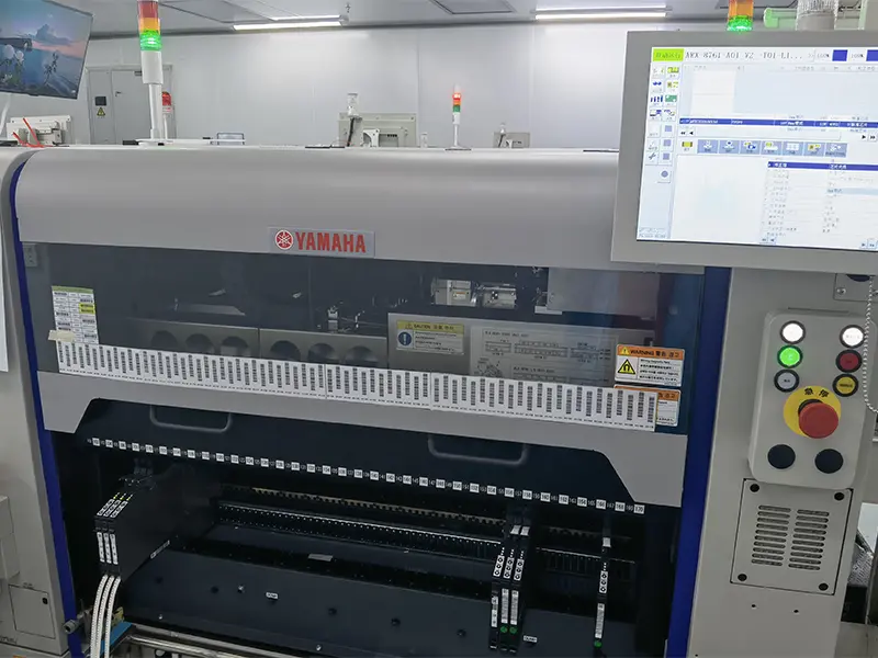
02. Yamaha Modular Placement
High-precision optical mounters executing ultra-fast pick-and-place down to 01005 passives and ultra-fine BGAs.
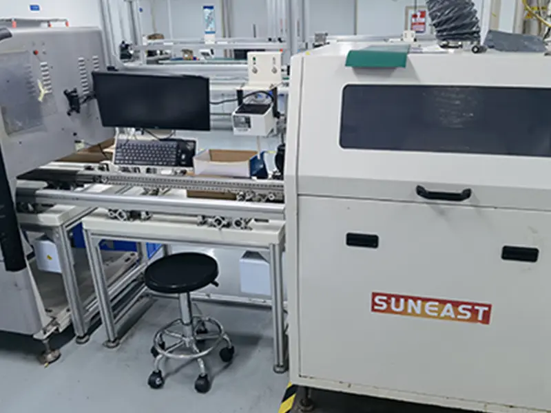
03. Pre-Reflow AOI Inspection
Catches component shift, skew, missing parts, or incorrect polarity before boards enter the reflow heat cycle.
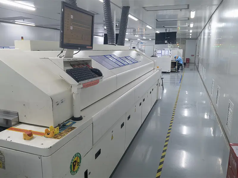
04. Nitrogen Reflow Profiling
Multi-zone precision temperature gradient tuning according to board thickness, layer count, and BGA mass.
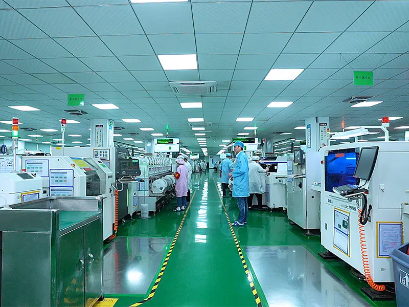
05. Controlled Clean SMT Hall
ESD-safe, temperature and humidity regulated cleanrooms preventing electrostatic discharge and moisture defects.
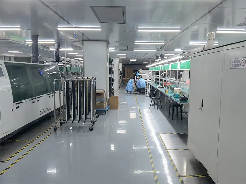
06. DIP Wave Soldering & Testing
Automated wave soldering, selective hand assembly, conformal coating, ICT bed-of-nails, and FCT test jigs.
Emerging Megatrends Reshaping PCB Fabrication & Turnkey Assembly
From AI hardware acceleration and mmWave 5G/6G communication to ultra-miniaturized medical wearables and electric vehicle power modules.
Edge AI & High-Compute Modules
Edge artificial intelligence microprocessors require extreme power density, ultra-tight decoupling capacitor placement, and high-layer count boards (16 to 32+ layers) with embedded microvias, back-drilling to eliminate stub reflections, and precise impedance tuning (±5%).
RF, Microwave & Radar Expansion
With anti-drone interceptors, phased-array radar, and commercial satellite constellations proliferating, low-loss dielectric laminates like Rogers RO4350B and Taconic with immersion gold finishes have become standard requirements for stable phase velocities above 500MHz.
EV Electrification & Heavy Copper
Electric vehicle battery management systems (BMS), high-voltage DC-DC converters, and industrial inverters demand heavy copper boards ranging from 4oz to 10oz finished copper, augmented by thermal aluminum backplanes capable of dissipating severe thermal loads.
Rigid-Flex Miniaturization
Smart health wearables and robotics demand rigid-flex assemblies that eliminate bulky wire harnesses and connectors. Stacking polyimide flex cores with FR-4 rigid zones enables compact 3D enclosure integration while maintaining dynamic flex fatigue endurance.
Target Application Domains & Specialized Process Windows
PCB ADEPT customizes thermal profiles, laminate stackups, and testing protocols according to distinct application stress profiles.
RF Telecommunications & Anti-Drone Systems
Low-loss hybrid stackups incorporating Rogers PTFE bonded with standard FR-4 prepregs. Hard gold or ENEPIG finishes prevent signal degradation on sensitive RF transmission lines, high-frequency antenna arrays, and high-power jamming amplifiers operating from 500MHz to 6GHz+.
Automotive BMS & Heavy Industrial Power
Heavy copper PCB assemblies (4oz to 10oz) optimized for continuous 100A+ current switching. Reinforced FR-4 with high glass transition temperatures (Tg 170°C–180°C), combined with selective wave-soldered power busbars, withstand severe automotive vibration profiles.
Medical Diagnostic & Biosensing Wearables
High-density interconnect (HDI) micro-via structures (1+N+1 to 3+N+3) utilizing laser-drilled blind and buried vias. Built to IPC-A-610 Class 3 medical standards, boards undergo 100% ionic contamination cleanliness testing to prevent dendrite growth in portable clinical hardware.
Featured PCB & PCBA Engineering Solutions (Part 2)
Explore our heavy copper, metal-core aluminum, multi-layer HDI, and rigid-flex product lines engineered for extreme durability, power density, and form-factor efficiency.
ODM China PCB Prototyping, Validation, and Manufacturing: Top Suppliers and Factory Solutions for Rapid Product Development Pricelist, Factories
Configure Specs
ODM High Density Interconnect PCB (HDI PCB) - Top China Suppliers & Factory for Advanced Circuit Boards Quotes, Pricelist
Configure Specs
Famous High Thermal Conductivity Aluminum PCB from China Suppliers and Factory - Ideal for Your Electronics Needs Companies, Factories
Configure Specs
High-Quality Heavy Copper PCB from China Suppliers: High Current Capacity for Power Converters and Vehicles | Factory Direct Quality Manufacturer, Supplier
Configure Specs
ODM China Suppliers Factory for Single and Double-Sided Rigid Flex PCBs, 4-16 Layer Complex Multi-Layer Solutions Pricelist, Factory
Configure Specs
High-Quality High-Quality Aluminum PCB from China Factory - Leading Suppliers for Thermal Management Solutions Pricelist, Factories
Configure Specs
Buy High Density Interconnect HDI PCB from China - Reliable Suppliers and Factory for Advanced Circuit Solutions Manufacturer, Pricelist
Configure Specs
China High Thermal Conductivity Aluminum PCB from Reliable China Suppliers | Quality Factory Manufacturing Supplier, Factory
Configure SpecsTrusted by Electronics Innovators Worldwide
Serving forward-thinking hardware startups, industrial instrumentation leaders, and aerospace pioneers across 50+ countries.










Frequently Asked Questions on PCB Prototyping & Turnkey Assembly
Direct technical answers addressing engineering prerequisites, quality inspection protocols, component sourcing strategies, and international delivery cycles.
What is your minimum order quantity (MOQ) for rapid PCB prototype assembly?
Our rapid prototyping service has an absolute MOQ of 1 piece up to pilot batch volumes of 500 pieces. Turnaround times typically range between 3 to 9 business days depending entirely on board layer complexity, laminate availability (standard FR-4 vs. high-frequency Rogers/Taconic), and special SMT component lead times.
Which specific design documentation is required to generate a definitive turnkey quote?
To avoid engineering delay, please furnish: (1) Gerber files in RS-274X format or native ODB++, (2) A consolidated Bill of Materials (BOM) in Excel format clearly indicating itemized Reference Designators, Manufacturer Part Numbers (MPN), descriptions, and acceptable alternate manufacturers, (3) Centroid / Pick-and-Place (X-Y coordinate) data, and (4) Fabrication and Assembly drawings detailing surface finish, copper weight, solder mask color, and specific testing or programming directives.
How does PCB ADEPT authenticate semiconductors and combat counterfeit parts?
We source active components exclusively through direct tier-1 factory-authorized distributors (e.g., Arrow, Avnet, Digi-Key, Mouser) and original component manufacturers (TI, ADI, STMicroelectronics, Microchip). All incoming lots pass through our strict IQC lab: undergoing high-magnification surface inspection, acetone chemical wipe tests to detect remarked packages, pin coplanarity checks, internal lead-frame X-ray analysis, and moisture barrier bag (MBB) sealing verification before kitting.
What inspection standards and testing methodologies are standard on SMT lines?
Every PCBA batch undergoes an end-to-end quality loop: (1) 3D Solder Paste Inspection (SPI) assessing solder paste volume, height, and bridging post-stencil, (2) Automated Optical Inspection (AOI) both pre-reflow and post-reflow, (3) First Article Inspection (FAI) verifying component values with an LCR meter against design schematics, (4) High-Resolution X-Ray Inspection (AXI) inspecting BGA, QFN, and bottom-terminated components for solder voiding (<15% IPC standard), and (5) Custom Functional Circuit Testing (FCT) utilizing engineering test jigs and client firmware.
Can you manufacture hybrid multilayer stackups combining FR-4 and Rogers PTFE materials?
Yes. We specialize in hybrid RF stackups combining high-frequency PTFE laminates (Rogers RO4350B, RO4003C, Taconic) with standard high-Tg FR-4 core and prepreg layers. This hybrid pressing architecture significantly reduces raw material costs while isolating high-speed RF microwave signal paths on outer layers, ensuring minimal dielectric loss (Df) and consistent relative permittivity (Dk) across ≥500MHz to 6GHz+ frequencies.
How do you support custom firmware programming, functional testing, and full box builds?
Our turnkey capabilities extend far beyond soldering bare circuit boards. We operate dedicated post-assembly cells supporting: IC offline/inline flashing (JTAG/SWD programming via Segger/custom jigs), conformal coating (acrylic, silicone, polyurethane) to protect against humidity/salt spray, high-temperature dynamic burn-in and aging chambers, plastic/metal enclosure mechanical integration, and final custom packaging labeled for direct retail distribution.
Initiate Your Turnkey Engineering Review
Send your native Gerber, ODB++, and BOM files directly to our senior engineering team in Shenzhen for a comprehensive DFM audit, impedance simulation, and factory-direct quotation within 2 to 4 business hours.