
China China PCB Prototype Suppliers: Fast-Track Your Product Development with Our Factory Solutions Manufacturer, Pricelist
Product Description
🚀 A Historical Perspective: The Evolution from "Months" to "Days"
Looking back at the history of the electronics industry, PCB manufacturing was once a lengthy and painful bottleneck.
💡 The Historical Lesson: Each technological advancement has compressed the time from "idea" to "physical object." This increase in speed has transformed product development from a serial, high-cost "gamble" into a parallel, low-cost process of "rapid iteration and failure."
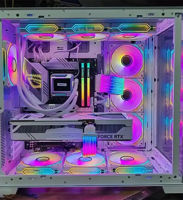

🔍 Rapid Prototyping and Product Validation
The value of rapid prototyping lies not just in its speed, but in how it empowers the entire validation process.
① Functional Validation
Verify circuit design correctness. Discover and fix schematic or component selection errors within days.
② Performance Validation
Assess signal integrity, power integrity, and EMC in high-frequency or high-speed applications early.
③ DFM/DFA Validation
Check component placement, spacing, and thermal management to prevent massive losses during mass production.
④ Mechanical Validation
Verify that PCB dimensions and connector positions perfectly match the product enclosure.
※ The Logic of Speed: Each rapid "design-prototype-validate" iteration eliminates a potential risk point. Shorter cycles allow more validation rounds, ensuring a smooth transition to mass production.
🛠️ Technological Advancements in Manufacturing
Modern rapid prototyping is enabled by several key technologies:

Laser Direct Imaging (LDI)
Uses lasers to image photoresist directly, offering high precision and adaptability for small-batch production.

Digital Workflows
AOI, flying probe testing, and automated handling minimize manual intervention and increase consistency.

High-Performance Materials
From standard FR-4 to Rogers high-frequency substrates and flexible PI, meeting diverse application needs.

Online Collaboration
Instant quotes and automated DFM analysis via Gerber file submission streamline the ordering process.
📋 Common PCB Types & Parameters
| Type | Name | Description | Key Parameters |
|---|---|---|---|
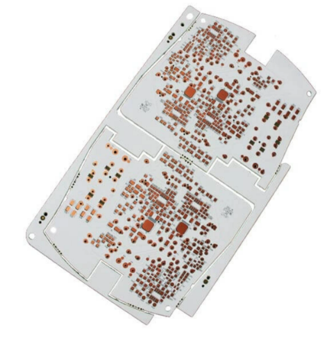
|
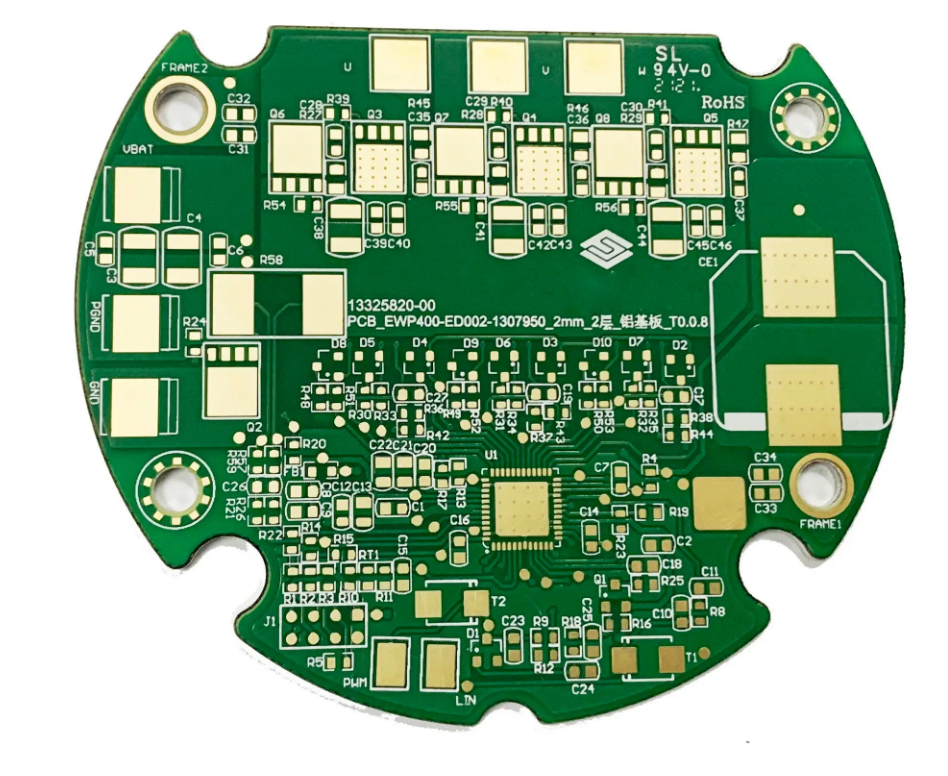
Single-Sided | Lowest cost, simple structure. Used in low-density electronics. | Thickness: 1.0-1.6mm Copper: 1oz Trace/Space: 0.2mm |
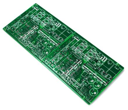
|
Double-Sided | Most common, routing on both sides. Standard electronics. | Thickness: 1.0-1.6mm Vias: ≥0.3mm Trace/Space: 0.15mm |
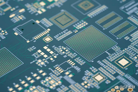
|
Multi-Layer | High density. Used in smartphones and industrial controls. | Layers: 4-12 Blind/Buried Vias Trace/Space: 0.1mm |
|
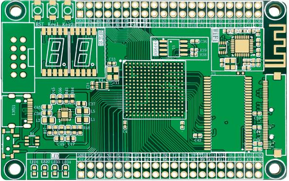
High-Freq./Speed | Low loss. Used in 5G, radar, and satellite communication. | Material: Rogers/Taconic Df Finish: ENIG |
|
HDI | High-Density Interconnect with micro-vias. For portable devices. | Laser Vias: 0.1mm Trace/Space: ≤0.075mm |
|
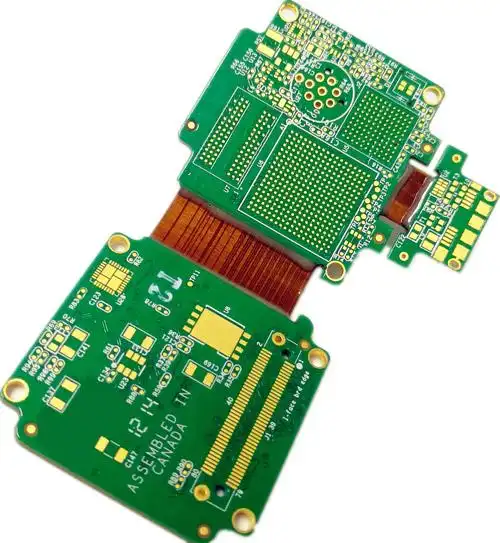
Flex/Rigid-Flex | Bendable, 3D assembly. Used in medical/wearables. | Substrate: PI Bend Radius: Critical |
📝 Conclusion
Rapid PCB prototyping has evolved from a supporting service into a strategic pillar of modern electronics innovation. It deeply embodies the modern R&D philosophy that "time is market, and validation is value." By mastering the process requirements for different PCB types, companies can build an efficient "design-validate-iterate" loop, seizing the initiative in a fiercely competitive market.









