
Flagship Hardware & Custom Manufacturing Platforms
Pre-engineered sub-assemblies, heavy copper systems, and quick-turn rigid-flex PCB fabrication pipelines available for rapid deployment and high-volume OEM replication.
Global Enterprise Procurement Dynamics for Rigid-Flex FPC
Analyzing modern SWaP-C optimization, reliability physics under high dynamic vibration, and how multi-layer rigid-flex circuitry replaces standard wire harness bottlenecks.
SWaP-C Optimization Pressures
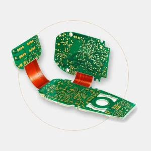
Global procurement teams across aerospace, handheld medical diagnostics, and next-gen military optics face extreme Size, Weight, Power, and Cost (SWaP-C) constraints. Discrete wire-to-board connectors represent mechanical failure liabilities and excessive mass. OEM rigid-flex circuits merge rigid FR-4/polyimide multi-layer zones with dynamic flexible polyimide ribbons, collapsing 3D volumetric envelopes by up to 60% while eliminating intermediate connectors completely.
Mean Time Between Failures (MTBF)
Cable assemblies, crimped pin terminals, and manual wire soldering introduce human error and failure points under shock and multi-axis mechanical vibration. Rigid FPC technology bonds the copper foil directly through adhesive-less or acrylic/epoxy lamination, ensuring unbroken electrical continuity. For Tier-1 automotive and industrial robotic motion joints, this continuous copper grain structure extends MTBF beyond 100,000 dynamic cycles.
Total Cost of Ownership (TCO) Shift
While bare rigid-flex boards exhibit a higher raw unit price than basic FR-4 slabs, sophisticated procurement engineering evaluates Total Cost of Ownership. By eliminating downstream hand assembly, wire stripping, crimping, wire-routing labor, and testing fixtures, overall bill-of-materials and assembly cycle times decline by 25% to 40%, yielding significant net financial and logistical savings over the product lifecycle.
Technical Architecture & Rigid-Flex Manufacturing Specs
Engineered to IPC-6013 Class 2 & Class 3 standards. Our Shenzhen production matrix integrates automated micro-drilling, plasma desmear, and high-precision vacuum hot-press lamination.
| Manufacturing Parameter | Standard Prototype Capability | Advanced OEM Production Window | Quality & Test Standard |
|---|---|---|---|
| Layer Count Combinations | 1–4 Flex Layers + 2–8 Rigid Layers | Up to 22 Multi-layer Stacks (Sequential Lamination) | IPC-6013 Type 4 Multi-layer Rigid-Flex |
| Base Flex Dielectric | Polyimide (PI) 12.5µm, 25µm, 50µm (Adhesive-less) | Cast Adhesiveless PI, Modified PI (MPI), LCP (Liquid Crystal Polymer) | IPC-4204/11 Low Moisture Absorption |
| Copper Foil Options | 1/3 oz, 1/2 oz, 1 oz Electro-Deposited (ED) | 1/3 oz to 3 oz Rolled Annealed (RA) Copper (High Dynamic Life) | IPC-4562 High Ductility Flex Copper |
| Min. Line Width / Space (L/S) | 0.075mm / 0.075mm (3.0 mil / 3.0 mil) | 0.035mm / 0.035mm (1.4 mil / 1.4 mil) via mSAP Semi-Additive | AOI Laser Optical Auto-Inspection |
| Microvia / Laser Blind Via | Mechanical Micro-via: 0.15mm (6 mil) | UV/CO2 Laser Drilled: 0.050mm (2 mil), Staggered & Stacked Via | Cross-section Microsectioning / IPC-TM-650 |
| Impedance Tolerance Control | ±10% Standard Single-Ended / Differential | ±5% Controlled Coplanar Waveguide & Stripline Across Transitions | Time Domain Reflectometry (TDR) 100% Tested |
| Stiffener Integration | FR-4, Polyimide (PI), Stainless Steel (SUS) | Aluminum (Thermal Dissipation), Ceramic, Laser-cut 316 Stainless | Bonding Peel Strength > 1.2 N/mm |
| Surface Finishes | Electroless Nickel Immersion Gold (ENIG) 1–3 µ" Au | ENEPIG (Wire-Bondable), Hard Gold Plating (Edge Connectors >30µ"), Immersion Silver | IPC-4552 / IPC-4556 Corrosion & Wetting Proof |
Macro Industry Solutions Powered by Rigid-Flex Engineering
From high-temperature automotive battery packs to mission-critical aerospace jamming equipment, our flexible and rigid circuits are built for rigorous deployment environments.
Automotive & EV Battery Management (BMS)
Electric vehicle battery modules demand ultra-flat cell sensing interconnects. Our rigid-flex designs incorporate NTC thermistors, voltage sensing nodes, and multi-pin BMS controller interfaces on a single monolithic flex circuit. This eliminates wire bundles, simplifies automated robotic pick-and-place pack assembly, and withstands continuous thermal shock from -40°C to +125°C under rigorous IATF 16949 conditions.
Aerospace, Avionics & Anti-Drone Systems
Electronic countermeasure (ECM) platforms, anti-drone directional jamming pods, and airborne radar assemblies operate within dense chassis with severe weight penalties. We deploy hybrid rigid-flex configurations pairing Rogers 4350B / Taconic PTFE RF layers with flexible polyimide interconnects. These configurations maintain phase consistency and ultra-low insertion loss across multi-gigahertz radar frequencies.
Medical Diagnostics & Surgical Endoscopy
Minimally invasive surgical instruments, ultrasonic catheters, and wearable patient telemetry demand bio-compatible, high-density flex circuitry capable of bending through tight articulating joints. Using rolled-annealed micro-copper and biocompatible polyimide covers, we produce sub-miniature flex interconnects down to 35µm pitch that withstand repeated sterilization and chemical exposure.
Industrial Automation & Multi-Axis Robotics
Continuous dynamic flex joints in industrial collaborative robots (cobots) suffer rapid fatigue failure when utilizing standard wiring. Our dynamic class-3 flex tails integrate tear-stop copper features, balanced neutral bending axes, and conductive carbon or silver EMI shielding to maintain signal integrity alongside multi-kW motor driver switching paths.
Engineering Roadmap: Rigid-Flex & FPC Innovation (2026–2030)
As computing workloads decentralize to edge AI nodes and photonics merge with electrical routing, circuit board manufacturing must evolve beyond traditional subtractive etching.
1. mSAP & Ultra-Fine Pitch Routing
Traditional subtractive chemical etching leaves trapezoidal trace side-walls, impairing high-frequency 5G/6G signal propagation below 50µm trace widths. Our active roadmap deploys Modified Semi-Additive Processing (mSAP), utilizing thin seed copper and electrolytic pattern plating to achieve vertical trace geometry with 15µm/15µm line/space resolutions. This supports next-generation wafer-level chip-scale packaging (WLCSP) directly on dynamic flex circuits.
2. Embedded Passive & Active Components
To further compress surface component real estate, inner-layer component cavities are being integrated directly into flexible polyimide cores. By burying thin-film resistors, decoupling capacitors, and bare silicon dies within the internal layers of a rigid-flex sandwich, external surface mount areas are freed entirely for high-pin-count processors, significantly lowering parasitic loop inductance for high-speed switching power converters.
3. Optoelectronic Hybrid Flexible Circuits
As serial data links approach 112 Gbps and 224 Gbps per lane in AI cluster backplanes, electrical copper traces encounter severe skin-effect losses. We are collaborating with photonics research partners to embed flexible optical polymer waveguides directly into multi-layer rigid-flex interconnects, allowing seamless electro-optical conversion without bulky external active optical cables (AOCs).
Commercial Dynamics, Shenzhen Turnkey Ecosystem & Compliance
Combining the world-class electronics component sourcing speed of Shenzhen's Bao'an industrial cluster with stringent international compliance frameworks.
The Shenzhen Advantage: Micro-Supply Chain Integration
Headquartered in the Anda Electronic Industrial Zone in Shenzhen, our manufacturing facility operates at the epicenter of global electronics production. Access to upstream raw laminate suppliers (Shengyi, Rogers, ITEQ, Doosan), dedicated laser-stencil tooling houses, and authorized distributors for TI, ADI, ST, Microchip, and Murata provides unparalleled turnaround speed. Where Western or fragmented supply chains require weeks just to consolidate raw flex materials, our local ecosystem accomplishes material kitting and precision DFM verification in 24 to 48 hours.
- Direct factory engineering communication (Zero broker overhead)
- In-house SMT assembly lines calibrated for 01005 passives and ultra-fine pitch BGAs
- Integrated box-build tooling, CNC enclosure machining, and custom test-jig fabrication
Localized Compliance, Export Protocols & IP Protection
For international buyers in North America, the European Union, and Australasia, supply chain compliance is non-negotiable. Our manufacturing and testing processes comply strictly with international safety, environmental, and material standards. Every customer design is governed by strict Non-Disclosure Agreements (NDAs), protected by centralized encrypted server architectures, and monitored through our transparent Manufacturing Execution System (MES).
- Environmental: Full compliance with EU RoHS 3 (Directive 2015/863) & REACH regulations
- Safety & Reliability: UL 94V-0 flammability certification, IPC-A-600 / IPC-A-610 Class 3 acceptance
- Traceability: Full material lot traceability with 100% C-of-C (Certificate of Conformance)
High-Reliability HDI, High-Frequency & Thermal PCBs
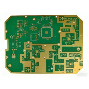
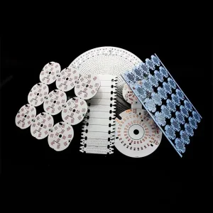
Explore specialized circuit solutions designed to complement complex rigid-flex assemblies, including high-thermal aluminum substrates and high-speed RF PCBs.
Frequently Asked Questions: Technical & Sourcing Authority
Comprehensive engineering clarifications addressing the most common search inquiries and technical specifications in OEM rigid-flex fabrication.
The minimum bend radius is strictly governed by whether the application is static (flex-to-fit during assembly) or dynamic (continuous flexing in motion systems). According to IPC-2223 guidelines, for static single-layer flex circuits, the minimum bend radius should be at least 6× the overall circuit thickness. For double-sided flex, this ratio increases to 10×. In multi-layer flex sections (3 or more layers), we recommend maintaining at least 20× the total thickness. For dynamic flex applications, the bend radius must exceed 20× to 40× thickness, and traces should always be placed on a single neutral mechanical bend axis using rolled annealed (RA) copper foil to prevent work-hardening and fatigue cracking.
Adhesiveless polyimide (cast or directly laminated copper onto polyimide) significantly outperforms adhesive-based laminates (which use modified acrylic or epoxy bonding layers). Adhesive layers possess a high coefficient of thermal expansion (CTE), especially along the Z-axis, which exerts severe mechanical stress on plated through-holes (PTH) and microvias during reflow soldering, leading to via barrel cracking. Furthermore, adhesiveless materials exhibit superior thermal resistance (Tg > 250°C), thinner overall stack-ups for tighter bend radii, reduced moisture absorption, and improved peel strength under prolonged thermal cycling.
Controlling characteristic impedance across rigid-to-flex transitions requires rigorous 2D/3D field-solver modeling (such as Polar SI9000). The dielectric constant (Dk) of rigid FR-4 typically ranges from 4.2 to 4.5, whereas flexible polyimide sits between 3.2 and 3.4, and coverlay film adhesives can vary between 2.8 and 3.5. To maintain continuous 50Ω single-ended or 90/100Ω differential impedance across the border, trace geometries (conductor width and coplanar gaps) must be adjusted at the transition interface, or cross-hatched reference copper planes must be calibrated to compensate for dielectric changes without sacrificing mechanical flexibility.
Electroless Nickel Immersion Gold (ENIG) is the industrial standard for SMT pads on rigid zones, providing excellent coplanarity for fine-pitch BGAs (0.4mm pitch) and 01005 passives. However, if the flexible extension serves as an edge connector or contact keypad subject to repeated mating cycles, ENIG gold (1–3 µ" Au) is too thin and brittle. In such cases, we deploy selective dual plating: electrolytic Hard Gold (>30 µ" Au over 100 µ" Ni) on contact fingers for wear resistance, and standard ENIG or ENEPIG (Electroless Nickel Electroless Palladium Immersion Gold) on SMT zones to avoid gold embrittlement in solder joints.
Polyimide is hygroscopic, naturally absorbing between 0.5% and 2.5% atmospheric moisture by weight. During lead-free reflow (peak temperature 245°C–260°C), trapped moisture vaporizes instantly, creating extreme internal vapor pressure that can cause catastrophic internal delamination or blister formation. We mandate a controlled pre-bake protocol prior to SMT assembly (typically 110°C–125°C for 4 to 8 hours depending on stack-up thickness and layer count). Boards are then processed through assembly within tightly controlled humidity chambers to maintain zero-defect surface mount assembly integrity.