
Featured Automated Circuit Board Assembly & Specialized Substrates
Explore our top-tier PCB and PCBA production lines engineered for high thermal conductivity, precision RF performance, and extreme-density multi-layer integrations.





Shenzhen ICSLOVE Technology (PCB ADEPT): Engineering Precision
Founded in 2020 in Bao'an District, Shenzhen, PCB ADEPT operates an 8,000 m² state-of-the-art facility featuring 6 automated SMT lines and 4 DIP wave soldering lines. We combine over 15 years of EMS and advanced substrate fabrication mastery to eliminate the friction between initial Gerber layout, procurement, pick-and-place mounting, and full box-build release.
Automated Circuit Board Assembly: Technology Roadmap & Future Outlook
Modern PCBA manufacturing is rapidly moving past standard surface-mount assembly. Our Shenzhen Smart Factory integrates artificial intelligence, real-time closed-loop optical feedback, and advanced metallurgy to satisfy hyper-dense edge-computing and extreme-environment aerospace demands.
Sub-01005 & Wafer-Level Packaging (WLP)
Integration of ultra-microscopic passive components down to 008004 formats and flip-chip die placement. Our dual-beam optical recognition and closed-loop linear motors achieve placement repeatabilities within ±0.015mm, critical for next-generation biometric implants and satellite transponders.
AI Closed-Loop 3D SPI & 3D AOI Symbiosis
Eliminating false calls and solder defects at the source: Our 3D Solder Paste Inspection systems communicate bi-directionally with high-precision stencil printers. Solder paste volume, height, and offset data trigger real-time auto-corrections to squeegee pressure, speed, and stencil wipe cycles.
Vacuum Soldering & Nitrogen Inerting
To resolve solder voiding in power MOSFETs, GaN FETs, and IGBT converters, our vacuum-assisted reflow modules lower chamber pressure to ≤10 mbar, pulling out volatile flux gases. Void percentages are maintained well below 5%—vastly surpassing standard IPC-A-610 Class 3 thresholds.
Embedded Component & Cavity Substrates
Shrinking PCB real estate by sinking capacitors, inductors, and bare dies directly into inner substrate cavities. Combined with Any-Layer HDI (up to 4x lamination) and hybrid Rogers-FR4 bonding, this architecture slashes parasitic inductance and delivers unmatched high-frequency signal integrity.
Macro Industry Solutions: Reliability Across Harsh Environments
Every sector presents distinct failure mechanisms—from thermal dissipation bottlenecks in industrial inverters to severe vibration and dielectric losses in anti-drone jamming arrays. Discover our customized manufacturing recipes.
Power Electronics & High-Current Inverters
Power converters require intense thermal pathways. We fabricate heavy copper boards (3oz up to 10oz+) paired with thermal vias and aluminum substrates, running automated selective soldering to guarantee complete barrel fill on high-amperage THT terminals.
RF, 5G/6G & Microwave Systems
High-speed telecommunications and radar electronics mandate strict dielectric tolerance and minimal passive intermodulation (PIM). We process high-frequency laminates (Rogers RO4350B, RO3003, Taconic) with micro-controlled impedance (±5%) and immersion ENEPIG finishes.
Automotive E-Mobility & High-Tg Electronics
Automotive BMS and powertrain ECUs must withstand intense thermal shock (-40°C to +150°C). We deploy high-Tg laminates (Tg170°C to Tg300°C) with automated conformal coating and 100% Automated X-Ray Inspection (AXI) to prevent hidden solder micro-cracks.
Anti-Drone & Aerospace Defense Arrays
Electronic warfare and counter-UAS platforms require high RF amplification without parasitic signal distortion. Our SMT mounting includes automated RF shielding can placement, thermal interface material dispensing, and full-spectrum functional RF testing.
Medical Implants & Diagnostic Wearables
From biocompatible wearable cardiac monitors to clinical laboratory analyzers, we build ultra-dense rigid-flex boards (1-6 flex layers, 4-22 rigid-flex layers) with bio-safe no-clean fluxes and 100% ionic contamination cleanliness testing.
Industrial Automation & Edge AI IoT
Harsh factory shop floors demand vibration resistance and extended product lifecycles. We support reverse engineering for legacy automation boards, long-lifecycle BOM planning, and automated bed-of-nails In-Circuit Testing (ICT) with programmed burn-in aging.
China Factory 4.0: Ecosystem Agility & Sourcing Dominance
While Western electronics contract manufacturers face lead-time paralysis and component shortages, Shenzhen offers an unprecedented micro-ecosystem where bare boards, passives, semiconductors, and specialized mechanical tooling are sourced and verified within a 1-hour radius.
The 1-Hour Bao'an Electronic Cluster
Located in Fuhai Subdistrict, Bao'an, PCB ADEPT sits at the geographic center of the world's most concentrated electronics supply chain. Bare PCB panels, laser-cut electro-polished stencils, and custom packaging arrive at our receiving docks within hours, enabling real 48-hour turnarounds for complex multi-layer prototypes.
Franchised Tier-1 Sourcing & BOM Reductions
Our 10+ year veteran procurement division maintains direct supplier relationships with original semiconductor manufacturers and authorized tier-1 global distributors (Arrow, DigiKey, Mouser, Avnet, and direct Asian factories for TI, ADI, ST, Microchip, Murata, and TE Connectivity), netting 10%–25% pure cost-down on high-volume runs.
End-to-End MES Traceability Architecture
Every incoming component reel receives a unique 2D barcode logged into our Manufacturing Execution System. As panels move across Yamaha pick-and-place feeders and reflow zones, our MES records operator IDs, oven temperature logs, machine placement parameters, and post-AOI inspection records, providing transparent audit trails for overseas OEMs.
Localization Support & Global Compliance Assurance
Partnering with a Chinese manufacturer shouldn't introduce legal or quality friction. We bridge continents through full IPC Class 2/3 manufacturing standards, RoHS/REACH environmental compliance, bilingual engineering account executives, and airtight Non-Disclosure Agreements (NDAs).
IPC-A-610 Class 2 & Class 3 Workmanship
Our assembly lines operate strictly under IPC-A-610 (Acceptability of Electronic Assemblies) and IPC-J-STD-001 (Requirements for Soldered Electrical and Electronic Assemblies). Dedicated quality engineers inspect barrel fill, fillet heights, solder wetting, and component skew to prevent field failures.
RoHS 3, REACH & UL94V-0 Certifications
All incoming raw laminates and solders are tested to conform to European Union RoHS 3 (Directive 2015/863) and REACH (EC 1907/2006) regulations, prohibiting hazardous lead, mercury, cadmium, and phthalates. Bare boards carry the UL94V-0 flammability certification stamp for overseas safety approval.
Bilingual DFM Support & IP Protection
Eliminate communication lag: our Shenzhen-based project engineers speak fluent technical English, providing Design for Manufacturability (DFM) and Design for Testing (DFT) reports within 12 hours of Gerber upload. Strict mutual NDAs and siloed data servers protect your proprietary firmware and schematics.
Global DDP Door-to-Door Logistics
We take complete accountability from our factory floor to your warehouse. Our international logistics department handles custom documentation, export clearance, import duties, and VAT under Delivered Duty Paid (DDP) terms via FedEx, DHL, UPS air express, or scheduled ocean freight.
Global Enterprise Procurement Guide: Automated PCBA Pricelist Matrix
Understanding contract electronics manufacturing pricing requires clear visibility into bare board fabrication, SMT machine setup (NRE), component placement per joint, and testing overhead. Below is our baseline pricing schedule for overseas procurement teams.
1. Volume Tier Turnkey Assembly Benchmark (Excluding BOM Components)
| Production Tier | Order Volume | Standard Lead Time | SMT Setup / NRE Fee | SMD Solder Joint Rate | First Article Inspection | Typical Application |
|---|---|---|---|---|---|---|
| Prototype / R&D | 1 – 50 pcs | 3 – 5 Days (Fast-turn 48h) | $50 – $120 | $0.006 – $0.010 / joint | Included Free | Proof-of-Concept, EVT/DVT, Seed Funding |
| Pilot / Trial Run | 51 – 500 pcs | 5 – 8 Days | $80 – $150 | $0.004 – $0.007 / joint | Included Free | PVT Testing, Field Trials, Regulatory Audits |
| Mid-Volume Production | 501 – 5,000 pcs | 10 – 14 Days | Waived (Rebate) | $0.0025 – $0.004 / joint | Included Free | Commercial Launch, High-Growth Hardware |
| High-Volume Enterprise | 5,000+ pcs | 14 – 18 Days | Waived (100% Free) | $0.0015 – $0.0025 / joint | Included Free | Mass Market OEM, Continuous Scheduled Releases |
2. Detailed Assembly Cost per Component Type & Secondary Processes
| Component Package / Process Type | Complexity Level | Cost per Joint / Point | Inspection Technology Applied | Quality Acceptance Criterion |
|---|---|---|---|---|
| Standard Passives (0402, 0603, 0805, 1206) | Standard SMT | $0.0020 – $0.0035 | 3D Solder Paste Inspection + 3D AOI | IPC-A-610 Class 2 / Class 3 |
| Micro Passives (0201, 01005) | High Precision | $0.0040 – $0.0065 | High-Mag Dual Beam 3D AOI | Zero Tombstoning, Exact Centering |
| Leadless ICs (QFN, DFN, LGA) | Advanced SMT | $0.0080 – $0.0150 | Automated Optical + X-Ray Sampling | <10% Solder Voiding Rate |
| Fine-Pitch BGA / CSP (≤0.5mm Pitch) | Complex SMT | $0.0150 – $0.0350 | 100% 3D Automated X-Ray (AXI) | 100% Ball Co-planarity & Void <5% |
| Through-Hole Wave Soldering (DIP) | Automated THT | $0.0120 – $0.0220 | Bottom-side AOI + Manual Inspection | >75% Through-Hole Barrel Wetting |
| Precision Hand Soldering / Flying Leads | Manual Specialized | $0.0350 – $0.0800 | High-Power Stereo Microscopy | IPC-J-STD-001 Certified Technicians |
| Automated Conformal Coating (Silicone / Acrylic) | Protection Process | $0.40 – $1.20 / board | UV Blacklight Film Inspection | Thickness 25μm – 75μm Uniform Coating |
| Firmware Flashing & Custom FCT Testing | Electrical Verification | $0.25 – $0.85 / board | Bed-of-Nails Automated Test Rig | 100% Pass Log Recorded to MES |
Turnkey Quotation Formula: Total Transparent BOM Breakdown
Total Project Cost = [Bare PCB Fabrication] + [Direct Component Sourcing Cost + 0%~5% Procurement Fee] + [Laser Stencil & Setup NRE] + [Placement Joints × Unit Rate] + [Custom Testing / Conformal Coating] + [Air Freight Shipping]. No hidden fees. Instant DFM feedback within 12 hours.
Step-by-Step Production Quality Control Pipeline
Take a photographic walkthrough of our Shenzhen SMT & DIP lines. Every single station feeds live data into our MES database, enabling serial-level traceability from raw component reel to delivered assembly.

Incoming Quality Control (IQC)
Every reel, tube, and tray of ICs undergoes rigorous pin-integrity verification, date-code checks, and anti-counterfeit testing before entering our moisture-controlled clean storage.
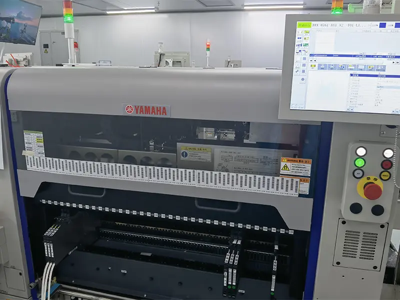
YAMAHA High-Speed SMT Placement
6 dual-lane YAMAHA placement lines mount passives down to 01005 and multi-lead BGAs with precision vision alignment and high-speed feeder systems.
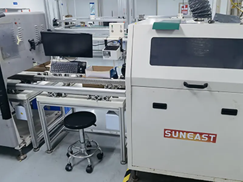
Pre-Reflow 3D Optical Inspection
Catches part orientation, component polarity, missing passives, and solder paste offset prior to entering the oven, ensuring 100% defect correction without thermal rework.
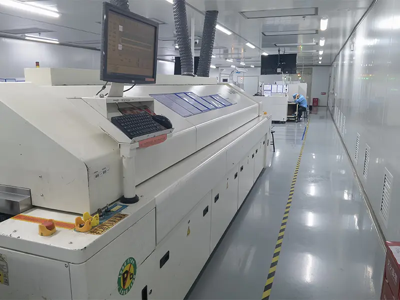
Multi-Zone Lead-Free Reflow Oven
10-zone nitrogen-purged reflow tunnels generate custom thermal curves matching board mass, heavy copper planes, and temperature-sensitive silicon requirements.
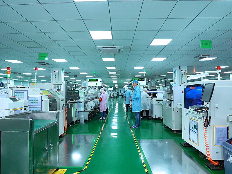
Class 100k Clean SMT Workshop
Temperature, humidity, and ESD-controlled shop floors ensure sensitive CMOS sensors, MEMS gyroscopes, and ultra-fine micro-BGAs are protected against electrostatic discharge.

Integrated Automated SMT Line
From automatic board de-stacking and inline stencil jet-printing to dual-stage post-reflow 3D AOI, the line operates seamlessly under continuous barcode supervision.
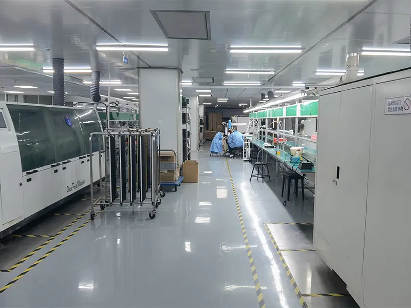
4 DIP Through-Hole & Wave Lines
Dedicated through-hole lines equipped with automated dual-wave soldering and robotic selective soldering arms handle heavy inductors, relays, and power terminal blocks.
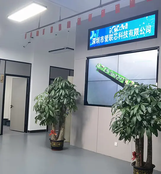
Box Build & Finished Product Integration
Complete mechanical enclosure assembly, CNC customized brackets, silicone gasket potting, ultrasonic plastic welding, final functional test, and custom retail packaging.
PCB Fabrication & Assembly: Engineering Parameter Summary
A comprehensive reference table for hardware design engineers, sourcing directors, and quality auditors vetting PCB ADEPT's production boundaries.
| Capability Category | Standard Production Envelope | Advanced / Custom ODM Limits |
|---|---|---|
| Rigid PCB Layers | 1 – 8 Layers (FR-4 Standard) | Up to 60 Layers (IPC Class 3, Heavy Copper) |
| Flex & Rigid-Flex Layers | Flex 1 – 2 Layers, Rigid-Flex 4 – 8 Layers | Rigid-Flex up to 22 Layers, Any-Layer HDI (4x) |
| Substrate Base Materials | Shengyi S1000-2, IT180A, Kingboard, FR-4 | Rogers (RO4350B, RO3003), Taconic, Megtron 6, Aluminum / Copper Base |
| Copper Foil Thickness | 0.5 oz – 2 oz (Outer / Inner) | Heavy Copper 3 oz – 12 oz (Continuous High Current) |
| Minimum Line / Spacing | 3.5 mil / 3.5 mil (0.09mm) | 2.5 mil / 2.5 mil (0.063mm with mSAP process) |
| Minimum Drill Hole Size | 0.20 mm (Mechanical Drill) | 0.075 mm (Laser Microvia for HDI) |
| Surface Finish Chemistry | HASL Lead-Free, Standard ENIG (Gold 1-2 μ") | Hard Gold (up to 50 μ"), Immersion Silver/Tin, ENEPIG, OSP |
| SMT Passive Component Range | 0402, 0603, 0805, 1206, SOD, SOT | Micro 0201, Ultra-Micro 01005 Chip-Scale |
| SMT IC & BGA Placement | SOP, QFP (0.5mm Pitch), BGA (≥0.8mm Pitch) | Micro-BGA (≤0.3mm Pitch), POP (Package on Package), QFN, LGA |
| Inspection & Verification | Visual QA, 2D AOI, Pre-reflow Optical | 3D SPI, Inline 3D AOI, 100% 3D AXI (X-Ray), Flying Probe, Bed-of-Nails ICT |
| Turnaround & Lead Time | Standard Turnkey: 5 – 9 Days | Fast-Turn Prototype: 48 – 72 Hours (24/7 Shift Mode) |
| Quality Standards & Auditing | ISO 9001:2015, RoHS 3, REACH, IPC-A-610 Class 2 | IPC-A-610 Class 3, UL94V-0, IATF 16949 Equivalent Controls, MES Lot Tracking |
Frequently Asked Questions: Procurement & Technical Reference
Comprehensive, straightforward answers addressing design file packages, counterfeit component prevention, BGA solder voiding, testing protocols, and DDP international shipping.
What is the minimum order quantity (MOQ) for prototype PCBA?
Prototype and trial-run PCB assembly starts from 1 piece and covers quantities up to around 500 pcs, with a typical lead time of 3–9 days depending on board complexity and component availability. We specialize in fast-turn R&D proof-of-concept builds without penalizing small orders with punitive minimum setup fees.
Which engineering files are required for an accurate turnkey quotation?
Send Gerber files (RS-274X format or modern ODB++), a complete Bill of Materials (BOM) in Excel with exact Manufacturer Part Numbers (MPN) and approved manufacturer names, a pick-and-place centroid file (XY coordinates and rotation), and assembly drawings. Test instructions, firmware binaries, or schematics are needed if you require MCU programming or functional circuit testing (FCT).
How does PCB ADEPT control PCBA quality and prevent solder defects?
Quality is controlled at every stage: IQC for incoming materials, 3D SPI for solder paste volume, pre-reflow optical inspection to eliminate part offset, 10-zone controlled reflow profiles, post-reflow dual-stage 3D AOI, First Article Inspection (FAI) with digital LCR verification, and 100% Automated X-Ray Inspection (AXI) for BGA/QFN packages. Every batch is recorded in our Manufacturing Execution System (MES) under our certified ISO 9001 quality system.
Can you source authentic components from brands like TI, ADI, ST, and Microchip?
Yes. Our dedicated sourcing team brings over 10 years of experience procuring original parts from franchised master distributors and factory-direct channels including Texas Instruments, Analog Devices, STMicroelectronics, Microchip, Murata, and TE Connectivity (Tyco). We maintain an internal safety inventory of common passives and propose qualified form-fit-function alternative parts whenever lead-time or cost poses a supply-chain risk.
What international certifications does PCB ADEPT hold?
Our manufacturing plant operates under an ISO 9001:2015 quality management system. Bare PCBs and turnkey assemblies are produced strictly to UL94V-0 flammability standards and comply fully with European Union RoHS 3 (Directive 2015/863) and REACH requirements for lead-free, non-toxic electronics assembly.
Do you offer box build, plastic enclosure molding, and finished assembly?
Yes. Beyond bare board assembly, our 8,000 m² factory supports plastic injection molding, CNC precision aluminum milling, 3D printing rapid prototyping, cable harness integration, memory and MCU firmware flashing, potting and conformal coating, thermal chamber burn-in aging, retail packaging, and worldwide DDP delivery.
How do you detect BGA solder voids and bridging on hidden pads?
Because optical cameras cannot inspect solder joints underneath Ball Grid Array (BGA), Quad Flat No-Lead (QFN), and Land Grid Array (LGA) components, we utilize high-resolution 3D Automated X-Ray Inspection (AXI). Our X-ray system calculates void percentage per solder ball, checks ball diameter uniformity, and detects micro-bridging or solder balling with automatic pass/fail thresholding.
What are your specific DFM rules for heavy copper boards in power converters?
For heavy copper boards (3oz up to 10oz+), etching lateral undercut requires increased trace spacing. We recommend minimum spacing of 10 mil for 3oz copper, and up to 20 mil for 6oz copper. In assembly, thermal relief pads on high-current planes must be designed with sufficient web widths, and selective soldering parameters must be adjusted for higher thermal sink capacity to achieve >75% barrel fill.
How do you prevent counterfeit or refurbished semiconductors from entering the lines?
We enforce a strict 4-tier anti-counterfeit protocol: 1) Sourcing exclusively from original component manufacturers (OCM) and franchised distributors; 2) Barcode and packaging verification against manufacturer datasheets; 3) Visual microscopic inspection of pin finishes, surface blacktopping, and laser marking indentation; 4) Destructive de-capsulation and electrical curve tracing whenever high-risk spot market parts are procured under client authorization.
How does PCB ADEPT handle intellectual property (IP) and data security?
We execute standard mutual Non-Disclosure Agreements (NDAs) enforceable internationally prior to receiving customer CAD databases. Gerber files and firmware binaries are stored on isolated, encrypted internal servers accessible only by assigned project engineering personnel. Programming stations are locked with hardware dongles to prevent unauthorized firmware copying.
What are your standard payment terms and international shipping options?
For initial prototype orders, standard terms are 100% T/T or credit card via secure portal upon order confirmation. For established production clients, we extend net-30 terms subject to credit review. We ship worldwide via FedEx, DHL, and UPS air express (3–5 business days transit) with Delivered Duty Paid (DDP) options that cover all customs duties and brokerage fees.
Can you support urgent fast-turnaround assembly in 48 to 72 hours?
Yes. If parts are consigned by the client or sourced from our pre-stocked in-house common component library, our Shenzhen factory can manufacture bare PCBs in 24 hours and complete precision SMT mounting, reflow, and testing within an additional 24–48 hours under our 24/7 dedicated fast-turn engineering shift mode.
Specialized High-Frequency, HDI & Rigid-Flex Circuit Solutions
Browse our extended catalog of advanced printed circuit board manufacturing solutions designed for RF signal integrity, rapid prototyping, and high-density space-constrained enclosures.




