
1 / 1
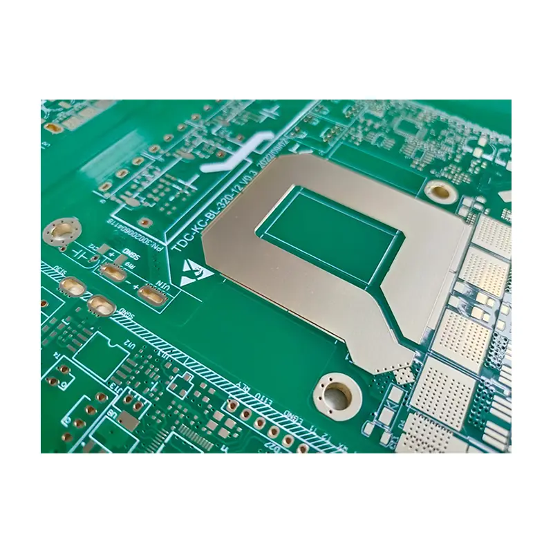
High-Quality Heavy Copper PCB Manufacturers in China - Reliable Suppliers for Power Converters with Excellent Heat Dissipation Suppliers, Factories
Product Description
What is Heavy Copper PCB?
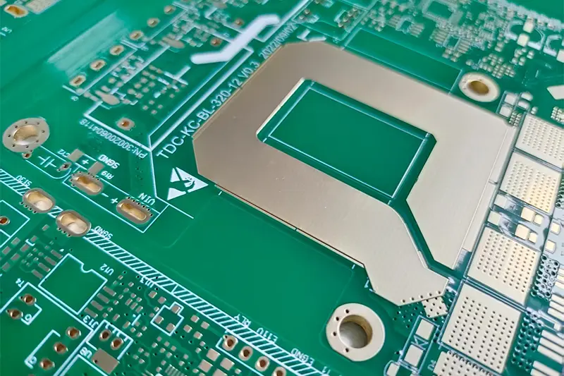
Core Purpose: Heavy copper PCB is engineered specifically for high-current and high-power applications (including power supplies, new energy systems, and industrial control equipment). Its primary structural advantages, design considerations, and applications are outlined below.
Core Features and Application Scenarios
Core Advantages
- Strong current-carrying capacity: The current-carrying capacity of 70μm copper foil (2 oz) is approximately twice that of 35μm copper foil (1 oz) at the same line width.
- Superior heat dissipation: The heavy copper layer rapidly conducts and spreads heat, minimizing thermal stress and overheating risks.
- High mechanical strength: Heavy copper thickness reinforces structural integrity, enhancing resistance to bending and mechanical shock.
Typical Applications
- Power converters (AC-DC / DC-DC)
- Battery Management Systems (BMS) for new energy vehicles
- Industrial frequency converters and motor drives
- Control modules for high-power welding machinery
Key Design Points
1. Selection of Copper Foil Thickness
- Common Specifications: 70μm (2 oz), 105μm (3 oz), 140μm (4 oz), extending up to 420μm (12 oz) for extreme power requirements.
- Scenario Matching: Select 2 to 4 oz copper for high current (≥5A) circuits. For extreme power loads (≥20A), implement 6 to 12 oz copper layers.
2. Trace and Current-Carrying Capacity Design
- Current-Carrying Calculation: Must balance copper weight, conductor width, and thermal limits (typically calculated for a 10°C temperature rise).
- Formula Reference:
I = K × W × T0.83
(Where I = current, K = thermal coefficient, W = line width, and T = copper thickness).
Example: A 2 oz (70μm) trace with a 5mm width yields approximately 15A carrying capacity at a 10°C temperature rise. - Trace Optimization: Keep high-current paths as short and wide as possible. Avoid abrupt line-width reductions ("narrow necks") to prevent localized thermal bottlenecks.
- Multi-Layer Parallel Routing: Distribute heavy loads across multiple connected copper layers in parallel (e.g., dual 2 oz layers provide equivalent conduction to a single 4 oz layer).
3. Via and Pad Design
- Vias: Enlarge via diameters for high-current conduction (≥0.5mm), increase total via count (rated around 1A per hole), and maintain barrel plating wall copper thickness of ≥20μm (compared to 8–12μm in standard PCBs).
- Pads: Heavy copper pads require an expanded surface area (0.2 to 0.5mm larger than standard footprints) to counteract rapid heat dissipation during soldering and eliminate cold joint risks.
4. Heat Dissipation and Insulation Design
- Thermal Dissipation: Dedicate heavy copper sections as embedded copper heat sinks, or implement dense arrays of thermal vias (pitch ≤1mm) tying into dedicated thermal planes.
- High-Voltage Isolation: Expand minimum clearance between heavy copper tracks (e.g., minimum spacing ≥0.2mm for 70μm copper) to eliminate electrical breakdown and creepage risks.
Manufacturing Process Difficulties and Control
1. Lamination & Etching
- High-Pressure Lamination: Executes under high-temperature/pressure conditions (180°C / 4MPa) to ensure bond strength between copper foil and core substrate (≥1.2N/mm).
- Etching Control: Due to slower etch rates (approx. 1μm/min), precise duration control is necessary to restrict undercut and side etching (≤0.05mm). Multi-stage stepwise etching prevents line-width deviations.
2. Warpage Control
- Thermal Expansion Matching: The significant CTE mismatch between heavy copper and FR4 requires a strictly symmetrical stackup (equal copper distribution on opposite layers).
- Structural Flatness: Include rigid intermediate cores to curb thermal warping within standard tolerance (warpage factor ≤0.5%).
3. Surface Treatment
- Finish Selection: Heavy copper is vulnerable to oxidation. High-temperature immersion tin or ENIG (Electroless Nickel Immersion Gold) is advised over standard OSP.
- Solder Mask Clearance: Pad openings must be strategically expanded to ensure complete solder wetting and secure intermetallic bonding over thick copper edges.
Core Summary
The cornerstone of heavy copper PCB engineering is high current-carrying capacity paired with efficient heat dissipation. Board designs must accurately calculate trace dimensions against thermal thresholds, while manufacturing protocols must overcome extended etching cycles and board warpage. These characteristics make heavy copper the premium solution for demanding industrial automation, automotive electronics, and renewable energy systems.
Frequently Asked Questions
What defines a "Heavy Copper PCB"?
A PCB is generally classified as a heavy copper (or thick copper) board when it features copper weights of 2 oz/ft² (70μm) or higher on inner or outer layers, going all the way up to 12 oz or more in extreme industrial designs.
What are the primary thermal advantages of heavy copper boards?
Heavy copper planes act as internal thermal conduction surfaces, dissipating heat away from high-power components and eliminating the need for expensive secondary heat sinks or noisy cooling fans.
Why is trace spacing larger on heavy copper PCBs?
Because thick copper takes longer to etch chemically, etching chemicals work laterally as well as vertically. Wider spacing accommodates etching tolerances and prevents electrical shorting or arcing under high-voltage conditions.
How do heavy copper PCBs prevent thermal warpage?
Manufacturers preserve board flatness by adopting symmetrical layer stackups, balanced copper distribution, and high-performance base materials with matched coefficients of thermal expansion (CTE).
Can heavy copper and standard copper thicknesses be combined on one PCB?
Yes, differential copper constructions allow engineers to place heavy copper on specific power layers while retaining standard 1 oz copper on signal layers for fine-pitch routing.









