

High-Yield Manufacturing Solutions
Precision Fabrication & Rapid Assembly Portfolio (Set I)
Explore custom board-level fabrication and turnkey assembly options designed for mission-critical prototypes and rapid volume ramps.

Famous High-Quality RF & Microwave PCBs from China Suppliers - Precision Impedance Control for ≥500MHz Frequency Applications
Explore RF Solutions
China China Flexible PCB: Lightweight & Bendable Solutions from Top Suppliers and Factory for Consumer Electronics
Review Flex Specs
Buy China Rigid Flex PCB Suppliers - Single & Double-Sided, 4-16 Layer Multi-Layer Flex PCB Factory Supplier
Request Rigid-Flex
Famous Heavy Copper PCB from China Suppliers - Durable, High-Performance Components for Power Converters and Vehicles
View Heavy Copper
High-Quality China Rigid Flex PCB Suppliers | Single & Double-Sided, Multi-Layer Rigid Flex PCB Factory Quotes
Get Custom Quote
Buy High Density Interconnect PCB - Top China Suppliers & Factory for Innovative HDI Solutions Pricelist
Check HDI Parameters
High-Quality RF & Microwave PCB Manufacturing in China | Low Loss, High Signal Quality - Trusted Factory
Consult RF Engineers
Global Landscape & Value Analysis
The Global Strategic Imperative for Rapid Prototyping PCBA
In modern electronic product design, the speed of hardware iteration dictates market dominance. China's rapid PCBA ecosystem compresses month-long product development cycles into days.
Compressed Product Cycles
Global commercial electronics brands and deep-tech hardware startups face shrinking market windows. Conventional EMS models that require 8–12 weeks of NPI (New Product Introduction) gestation are no longer commercially viable. Rapid PCB assembly services bridge the critical gap between CAD validation and high-volume rollouts.
- Iterative firmware & hardware co-design validation
- Elimination of multi-vendor coordination overheads
- Pre-compliance testing without tooling commitments
Capital-Efficient Scaling
By engaging specialized Chinese rapid prototyping factories, Western OEM/ODMs eliminate substantial capital expenditure risks. Prototype PCBA batches (1–500 units) serve as pilot runs that uncover structural DFM/DFA defects, solder joint thermal stress anomalies, and trace impedance mismatches prior to expensive metal tooling and SMT steel stencil mass fabrication.
- Direct ROI through zero-setup-cost test runs
- Accurate BOM cost variance forecasting
- Seamless handoff to 100k+ mass assembly lines
Complex Mixed-Technology Assembly
Modern applications combine power electronics with micro-pitch computation and RF links. Prototyping demands an integrated factory footprint capable of executing multi-stage solder reflow, selective through-hole wave soldering, conformal coating, and fine-pitch BGA underfill on the exact same manufacturing floor without outsourcing intermediate steps.
- High-layer rigid-flex integration (up to 22 layers)
- Heavy copper (3oz–10oz) combined with micro passives
- Advanced RF hybrids (Rogers / Taconic / FR-4)
Engineering Insight: The "First Time Right" Principle in Fast Turnaround
True rapid prototyping is not solely about line velocity; it hinges on automated front-end engineering. Over 74% of prototype delivery delays originate from Gerber design mismatches, silkscreen-on-pad overlaps, and unverified BOM part number MPNs. Shenzhen ICSLOVE Technology (PCB ADEPT) executes full-scale DFM (Design for Manufacturability) and DFA (Design for Assembly) computational audits within 2 hours of file submission.
Unrivaled Supply Chain Clustering
Why China—and Specifically Shenzhen—Dominates Global PCBA Agility
Shenzhen's Greater Bay Area houses the world's most dense electronics supply ecosystem. This geographic concentration reduces procurement latency from weeks to hours.
1 Hour
BOM Component Sourcing Radius
24 Hours
Standard 2-4 Layer Bare PCB Turn
99.8%
First-Pass Assembly Yield Rate
15+ Years
Engineering Team Experience
Huaqiangbei & Centralized Hubs
Located in Bao'an District, Shenzhen, our facility operates within minutes of world-renowned active/passive component distributor hubs. Where overseas assemblers face international freight bottlenecks for hard-to-find ICs, our sourcing department acquires genuine, traceable components from authorized franchise channels (TI, ADI, STMicroelectronics, Microchip, Murata, TE Connectivity) within the same business day.
Dynamic BOM Cost-Down & Equivalence
Global supply chain volatility frequently causes unexpected obsolescence or 50+ week lead times for specialized microcontrollers and power management chips. Our engineering procurement specialists utilize real-time parametric databases to suggest pin-to-pin, functionally identical drop-in alternative components that preserve design intent while saving 10% to 30% in bill-of-materials cost.
Integrated SMT & DIP Under One Roof
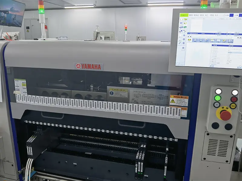
Our 8,000 m² factory integrates 6 high-speed SMT lines equipped with Yamaha mounters alongside 4 dedicated DIP through-hole and wave soldering lines. Keeping fabrication, laser stencil cutting, paste printing, automated component placement, thermal reflow, and full-spectrum testing enclosed in one controlled environment eliminates vendor-to-vendor freight damage and ensures 100% process traceability.
Precision Engineering Standards
PCB Fabrication & SMT Assembly Technical Roadmap
A rigorous DFM/DFA engineering reference documenting critical manufacturing tolerances, line capabilities, and quality thresholds for hardware architects.
| Process / Technical Parameter | Standard Rapid Capability | Advanced / High-Density Limits | Quality Inspection Verification Method |
|---|---|---|---|
| Layer Count (Rigid & Multilayer) | 1 – 8 Layers | Up to 60 Layers (IPC Class 3) | Automated Optical Inspection (AOI) & Microsection Analysis |
| Rigid-Flex & Flex Circuits | Flex: 1–6 Layers / R-F: 4–12 Layers | Rigid-Flex up to 22 Layers with HDI | Peel Strength Test, Bending Fatigue & High-Pot Testing |
| Smallest Component Placement | 0201 Imperial (0.6 × 0.3 mm) | 01005 Imperial (0.4 × 0.2 mm) | 3D Solder Paste Inspection (SPI) & Pre-Reflow AOI |
| Fine Pitch IC / BGA / CSP | 0.4mm pitch CSP / QFN | 0.35mm ultra-fine ball pitch BGA | High-Resolution 2D/3D X-Ray Inspection (AXI) |
| PCB Minimum Trace Width / Spacing | 3.5 mil / 3.5 mil (0.089 mm) | 2.0 mil / 2.0 mil (0.05 mm) HDI | Laser Direct Imaging (LDI) & AOI Trace Verification |
| Via Architecture | Through-hole, Mechanical Blind/Buried | Laser Micro-Vias, Any-Layer HDI, VIPPO | Thermal Shock Testing & Cross-Sectioning Inspection |
| Base Substrates Handled | Standard FR-4, Aluminum, Copper Base | Rogers 4350B, Taconic, PTFE, Polyimide | Material Certifications (IQC) & Dielectric Constant Validations |
| Surface Finishes | HASL Lead-Free, ENIG (Immersion Gold) | ENEPIG, Hard Gold Finger, Immersion Silver/Tin | X-Ray Fluorescence (XRF) Coating Thickness Measurement |
| Turnaround Speed (Prototypes) | 3 to 7 Days (Turnkey) | 24 to 48 Hours Express (Double-Sided) | Integrated MES Line Scheduling & Real-Time Milestone Tracking |
Field-Tested Reliability
High-Reliability Localized Application Domains
Our rapid prototyping services are engineered to meet stringent thermal, vibrational, and electromagnetic compatibility profiles across diverse verticals.
RF, Microwave & Anti-Drone Systems
Modern defense, wireless radar, and counter-UAS (anti-drone jamming guns) require flawless RF transmission paths with tight controlled impedance tolerances (±5% or ±7%). Prototypes leverage high-frequency Rogers laminates with tight thermal coefficient control and hybrid FR-4 pressings to minimize insertion loss up to 10 GHz+.
- Precision RF shielded enclosures and grounding vias
- High-power PA thermal sink copper coining
- Vector network analyzer (VNA) signal verification
Automotive, EV Power & BMS Controllers
Battery Management Systems (BMS), DC-DC converters, and motor inverters subject circuit boards to extreme currents and ambient thermal cycles. We assemble heavy copper PCBs (up to 6oz outer, 10oz inner) combined with aluminum heat sink cores, guaranteeing dissipation performance and solder fatigue resistance over thousands of thermal shocks.
- Thermal stress screening (-40°C to +125°C)
- High creepage and clearance safety routing
- Selective potting and conformal protective coatings
Medical Diagnostics & Wearable Health
Portable medical hardware, patient monitoring nodes, and wearable biosensors demand ultra-compact multi-layer rigid-flex interconnects and miniaturized 01005 passives. Assembled in ESD-safe cleanroom environments under ISO 9001 quality controls, each assembly provides complete lot traceability back to raw silicon and base prepreg lots.
- Zero-flux residue ultrasonic wash cleaning
- 100% 3D AOI inspection for micro-solder bridges
- Biocompatible potting and flex strain reliefs
Industrial Automation & Edge AI SBCs
Single-Board Computers (SBCs), Raspberry Pi industrial expansion HATs, and Programmable Logic Controllers (PLCs) integrate multi-core SoCs, high-speed DDR4/DDR5 memory routing, and dense Gigabit Ethernet magnetic interfaces. Rapid prototype verification ensures high signal integrity with zero bit-error rates under harsh factory floor EMI environments.
- Length-matched differential pair validation
- In-circuit firmware MCU flashing & boundary scan
- Turnkey customized CNC metal enclosure fitting
Full-Stack Quality Assurance
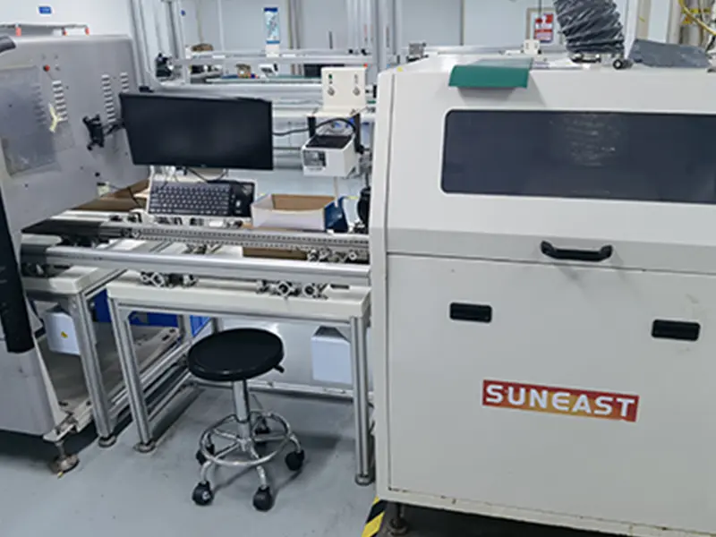
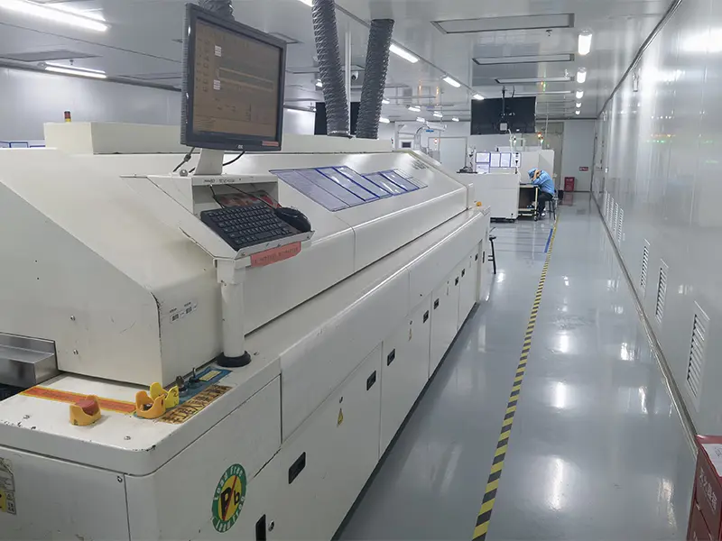
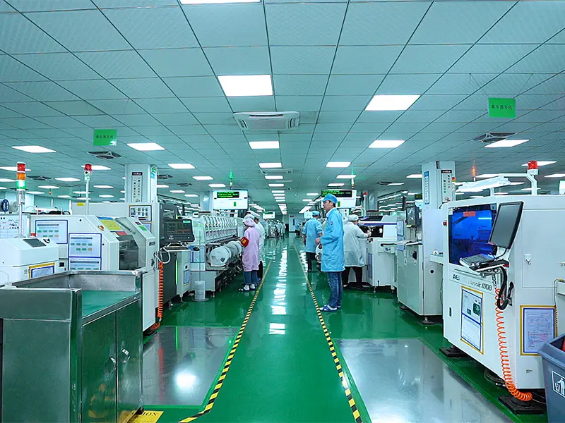
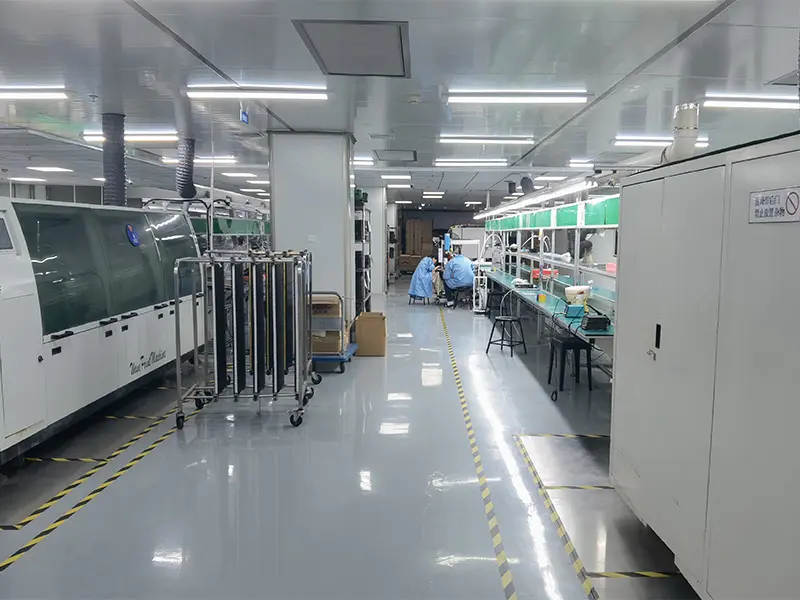
Inside the 8,000 m² Shenzhen Production Workshop
Take an operational look at the advanced equipment stations handling precision assembly, solder profiling, and optical analytics under ISO 9001 governance.

Export Compliance & Turnkey Box Build
Localized Support, International Certifications & Global Logistics
Eliminate procurement friction. We support overseas clients with native bilingual engineering communication, complete export customs compliance, and full box-build execution.
Dedicated English-Speaking Engineering
No lost-in-translation bottlenecks. Each project is assigned a designated Senior PCBA Project Engineer who reviews your schematics, Gerbers, and BOM in real time. We provide engineering query (EQ) sheets within 12 hours, highlighting part mismatches or package conflicts before lines are set up.
Full Turnkey Box Build Integration
Take your project beyond bare assemblies. We provide custom CNC aluminum machining, plastic injection tooling, rapid 3D printing prototyping, silicone keypad molding, cable harness assembly, MCU firmware flashing, serial number laser etching, and customized retail blister/box packaging.
Worldwide Door-to-Door DDP Logistics
We work directly with major logistics carriers (DHL Express, FedEx, UPS air express, and sea/air consolidators) handling customs declarations, export tariff codes, and certificates of origin. Prototypes manufactured in Shenzhen routinely reach engineering desks in North America and Europe within 3 business days of leaving our inspection bay.
Direct Engineering Responses
Frequently Asked Questions: Rapid PCBA Manufacturing
In-depth answers addressing design file packages, counterfeit mitigation, testing protocols, and intellectual property protection.
What exact design documentation is needed to initiate a 48-hour prototype assembly quote?
To achieve our fastest turnaround, please provide: (1) RS-274X or ODB++ Gerber files with drill data; (2) A complete Bill of Materials (BOM) in Excel format with columns detailing Item Number, Reference Designator, Manufacturer Part Number (MPN), Brand Name, Package/Footprint, and Quantity; (3) Pick-and-Place (Centroid / XY data) file exported from your EDA CAD tool (Altium, KiCad, Eagle, or Allegro); and (4) Assembly drawings indicating component polarity, fiducials, and any special assembly instructions (e.g., conformal coating keep-out zones).
How does PCB ADEPT guarantee 100% genuine components and prevent counterfeit silicon?
Our procurement protocols enforce strict supply chain vetting. We buy directly from original semiconductor manufacturers or Tier-1 franchised global and domestic distributors (including DigiKey, Mouser, Arrow, Avnet, and verified primary distributors in China). Our IQC laboratory verifies incoming lots using high-magnification optical microscopes to check marking authenticity, date code consistency, pin finish metallurgy, and packaging anti-static integrity. Certificates of Conformance (CoC) are retained for complete batch traceability.
Can you perform functional testing (FCT) and MCU firmware programming on rapid prototypes?
Yes. Beyond standardized SPI, AOI, and 3D X-Ray inspection, we routinely execute custom functional testing. Customers provide test fixtures (pogo-pin test jigs), firmware hex/bin binaries, and step-by-step test instructions. We flash microcontrollers (STM32, ESP32, PIC, Nordic, TI BLE chips), verify power rail voltages, test peripheral connectivity (USB, CAN, RS-485, Wi-Fi, BLE), and document test logs per serialized board before dispatch.
What are your minimum order quantities (MOQ) and sample lead times?
We have zero minimum order quantity (MOQ: 1 piece). We cater specifically to R&D engineering phases, functional prototypes, and small pilot production runs ranging from 1 to 500 boards. Typical turnkey lead time is 3 to 7 business days once component kitting is complete, with 24-to-48-hour express assembly options available for urgent hardware releases.
How do you safeguard client intellectual property and hardware designs?
We operate under stringent non-disclosure agreements (NDAs) signed prior to reviewing any technical files. All customer CAD files, Gerber archives, firmware binaries, and proprietary schematics are stored on isolated, encrypted internal servers with restricted departmental access. We never share customer artwork, showcase client boards without express written consent, or sell overstock production.
What soldering and PCB assembly standards are applied during production?
All surface mount and through-hole assembly processes strictly comply with IPC-A-610 Class 2 standards by default, with IPC-A-610 Class 3 (high reliability / mission critical) options available for medical, aerospace, and defense applications. Soldering follows J-STD-001 requirements utilizing lead-free RoHS-compliant SAC305 (Sn96.5Ag3.0Cu0.5) paste or specialized low-temperature alloys depending on component thermal sensitivity.
High-Yield Manufacturing Solutions
Precision Fabrication & Rapid Assembly Portfolio (Set II)
Advanced high-thermal aluminum substrates, single-board computer extensions, and heavy copper industrial circuit solutions.

Buy High Thermal Conductivity Aluminum PCB from China Suppliers - Reliable Factory Production Manufacturers
View Aluminum PCBs
High-Quality China Raspberry Pi HAT: Affordable Mini Single-Board Computer from Reliable Suppliers and Factory
Explore SBC Boards
Famous High TG PCB Suppliers in China - Durable Rogers PCBs for Automotive, Aerospace & Defense Industry
Review High TG Specs
China High-Density Interconnect PCBs from China | Trusted Suppliers and Factory for Quality HDI Circuit Boards
Request HDI Quote
Famous Heavy Copper PCB for Power Converters - Top China Suppliers & Factory for Strong Current Capacity
Inspect Power Boards
OEM High-Quality Flexible PCB from China Suppliers - Lightweight, Bendable and Foldable Solutions
Examine Flex Layers
Famous Heavy Copper PCBs from China Suppliers - High Current Capacity & Excellent Heat Dissipation Factory Solutions
Learn More