
High-Precision PCB & PCBA Product Portfolio
Direct manufacturer solutions engineered to bridge DigiKey-designed schematics with agile Shenzhen turnkey electronic manufacturing.

High-Quality Single & Double-Sided Rigid Flex PCBs
Multi-layer rigid-flex boards with dynamic bending endurance, polyimide flex cores, and FR-4 stiffening for dense aerospace and wearable form factors.
View Specifications
High Frequency PCBs for Low Signal Loss & EMI Suppression
Advanced Rogers and Taconic substrate fabrication with tight dielectric tolerance (Dk/Df control) to eliminate crosstalk in 5G and radar systems.
View Specifications
High Density Interconnect (HDI) Innovative Microvia PCBs
Laser microvia drilling (blind/buried vias), fine line pitch down to 2.5/2.5 mil, supporting 0.35mm pitch BGAs for next-gen IoT and telecom modules.
View Specifications
1–60 Layers Multilayer PCB Rapid 48h Turnaround
Massive multilayer capability featuring precise registration control, controlled impedance testing, and rapid dispatch for mission-critical industrial designs.
View Specifications
ODM High-Density Interconnect HDI PCB Solutions
Turnkey engineering integration, staggered microvias, stacked copper-filled vias, and high-frequency hybrid pressing for compact computing platforms.
View Specifications
ODM Rapid PCB Prototyping & Quick SMT Run
Expedited prototype manufacturing for hardware startups and enterprise labs. 24-hour PCB fabrication with 72-hour turnkey SMT component loading.
View Specifications
OEM High TG PCB (TG150–TG300) for Automotive & Defense
Glass transition temperatures up to TG300, delivering outstanding CAF resistance, dimensional thermal stability, and prolonged life under high under-hood heat.
View Specifications
Custom 4–16 Layer Rigid-Flex Integrated Assemblies
Optimized stack-up geometries eliminating wire harnesses, reducing assembly mass, and boosting signal integrity in robotics, drones, and medical probes.
View SpecificationsThe Global Commercial Paradigm of DigiKey PCB Assembly & Chinese EMS Manufacturing
In modern electronic hardware engineering, the workflow connecting electronic component catalog databases—such as DigiKey, Mouser, Newark, and Arrow—with contract printed circuit board assembly (PCBA) has become the de facto international benchmark for rapid innovation. Hardware engineers, embedded designers, and procurement managers worldwide rely heavily on DigiKey part numbers (DKPN) and manufacturer part numbers (MPN) during initial schematic capture and PCB CAD routing (Altium Designer, Cadence Allegro, KiCad, Mentor Xpedition). However, transitioning a prototype conceived in DigiKey into commercial mass production exposes acute friction points: single-piece component markups, inventory fragmentations, transatlantic shipping delays, and separate subcontracting of bare boards and surface-mount technology (SMT) assembly.
This is where Shenzhen ICSLOVE Technology Co., Ltd. (operating globally as PCB ADEPT) bridges the architectural gap. Operating from the heart of the global electronics capital in the Bao'an District of Shenzhen, our facility operates an intelligent, integrated turnkey manufacturing model. We combine native DigiKey BOM compatibility with the world's most dense electronic components supply chain ecosystem, offering global engineering firms institutional-grade assembly speed, traceable component sourcing, and drastic unit-cost reduction.
The Shenzhen Efficiency Multiplier: Transforming DigiKey BOMs into Scalable Production
For international buyers across North America, Europe, and the Asia-Pacific, ordering components directly from Western catalog distributors for full batch assembly incurs heavy logistics friction and prohibitive bill-of-materials (BOM) costs. A microcontroller or passive component reel that carries catalog retail pricing in the United States can frequently be procured directly through tier-1 franchised regional manufacturers in China at 20% to 50% lower unit costs, while maintaining identical silicon die integrity, manufacturer date codes, and factory warranties.
At PCB ADEPT, our engineering procurement specialists parse client BOM files with automated algorithmic cross-referencing. When an engineering team provides a BOM populated with DigiKey part references, our system immediately executes a three-tier analysis:
1. Direct Authorized Channel Verification: For proprietary chips (Texas Instruments, Analog Devices, STMicroelectronics, Microchip, NXP), we verify availability against authorized regional distributions to maintain full trace origin certificates.
2. Pin-to-Pin Drop-In Equivalency Modeling: Where passive components (Murata, TDK, Samsung, Yageo) or general-purpose discretes carry elongated lead times or catalog retail premiums, we provide certified parametric cross-matches with zero PCB pad layout changes.
3. Hybrid Supply Optimization: Clients can selectively consign rare or proprietary ICs directly from DigiKey to our factory while entrusting 95% of standard passives, connectors, and bare boards to our local ecosystem, compressing total lead time down to 3 to 9 business days.
Why Tier-1 Innovators Choose Our Shenzhen Assembly Center
A unified manufacturing ecosystem engineered to eliminate quality drift and vendor fragmentation.
Intelligent SMT Placement
6 high-speed automated YAMAHA and Panasonic SMT lines capable of placing 01005 passives, ultra-fine pitch 0.3mm micro-BGAs, QFNs, and POP (Package on Package) with sub-micron precision.
- Min Component: 01005 (0402 metric)
- BGA Pitch: 0.30mm with X-Ray inspection
- Placement Accuracy: ±0.025mm @ 3-sigma
3D SPI & 3D AOI Quality Gate
Every single printed board passes in-line 3D Solder Paste Inspection (SPI) prior to component mounting, followed by multi-angle 3D Automated Optical Inspection (AOI) post-reflow.
- 100% Volume & Height SPI verification
- 3D shadow-free height defect measurement
- First Article Inspection (FAI) reports included
End-to-End MES Traceability
Integrated Manufacturing Execution System (MES) links every serial number to reel lot codes, solder paste batch numbers, reflow thermal profiles, and individual inspection logs.
- ISO 9001:2015 audited quality governance
- Reel-level barcode scanning against BOM errors
- Lifetime traceability for industrial & medical lots
Comprehensive Box Build & Test
From bare circuit boards to factory-sealed turnkey products. We execute CNC machining, injection molding, MCU firmware burning, conformal coating, and custom packaging under one roof.
- Automated Functional Circuit Testing (FCT)
- High-temperature thermal burn-in aging chambers
- Robotic silicone & polyurethane conformal coating
High-Reliability Application Domains We Power Globally
From mission-critical aerospace modules to extreme-environment power distribution, discover how our assembly services execute against rigorous industry parameters.
RF, Telecom & Microwave Systems
Assembling multi-gigahertz baseband hardware, phased array antenna transceivers, and satellite downconverters using low-loss Rogers 4350B, Taconic, and high-frequency PTFE laminates with immersion silver or ENIG finishes.
Anti-Drone & Defense Jamming Electronics
Specialized high-power SMT with heavy copper heatsinks (up to 12oz) and automated void-free vacuum reflow soldering for RF power amplifier modules, ensuring zero hot spots during continuous broadband jamming operations.
Automotive Powertrain & BMS Electronics
Certified assembly for Electric Vehicle battery management systems (BMS), high-voltage DC-DC converters, and autonomous sensor suites engineered with high-Tg FR-4 (Tg170–Tg180) to survive severe thermal cycling (-40°C to +125°C).
Medical Instrumentation & Wearables
Miniaturized rigid-flex and HDI circuit manufacturing for diagnostic monitors, ultrasound probes, and wearable health sensors requiring biocompatible materials, cleanroom assembly standards, and IPC Class 3 joint reliability.
Industrial Automation & Edge AI Controllers
Ruggedized programmable logic controllers (PLCs), motor drivers, and industrial IoT gateway computers with conformal acrylic coating for harsh factory environments exposed to humidity, chemical fumes, and mechanical vibration.
Energy Storage & Solar Inverters
Thermal management circuit boards combining aluminum metal core baseplates (MCPCB) and heavy copper traces designed to handle massive surge currents (>100 Amps) with ultra-low thermal resistance.
PCB Fabrication & DigiKey SMT Assembly Capabilities
A comprehensive DFM engineering checklist designed for procurement leads, hardware engineers, and supply chain directors.
| Manufacturing Parameter | Standard Prototype Capability | Advanced Production Window | Verification / Testing Protocol |
|---|---|---|---|
| Layer Count | 1 to 8 Layers | Up to 60 Layers (Rigid), 22L (Rigid-Flex) | AOI optical inner-layer alignment check |
| Base Materials | Standard FR-4 (Tg140–Tg150) | Isola, Rogers, Taconic, Shengyi, Polyimide, Al/Cu Core | Incoming raw laminate XRF and TG validation |
| Min Trace Width / Spacing | 3.5 mil / 3.5 mil (0.088mm) | 2.0 mil / 2.0 mil (0.050mm) for HDI Any-Layer | Laser cross-section & etched copper measurement |
| Min Laser / Mechanical Drill | 0.20mm (Mechanical) | 0.075mm (UV Laser Microvia) | Plated through-hole (PTH) cross-section microscopy |
| Surface Finishes | HASL Lead-Free, ENIG (Electroless Nickel) | ENEPIG, Hard Gold (30u"), Immersion Tin / Silver, OSP | X-ray fluorescence (XRF) coating thickness test |
| SMT Component Envelope | 0402, 0603, 0805, SOIC, QFP | 01005 passives, 0.3mm micro-BGA, WLCSP, POP | High-magnification 3D SPI and post-reflow AOI |
| BGA Solder Void Control | < 15% Void Rate (IPC Class 2) | < 5% Void Rate with Vacuum Reflow (IPC Class 3) | High-resolution 2D/3D X-Ray Computed Tomography |
| Component Procurement | Consigned BOM parts from DigiKey/Mouser | Full Turnkey sourcing (Franchised Direct + DigiKey API) | 100% IQC inspection (microscopy, pin test, LCR) |
| Testing Services | Visual + First Article Inspection | Bed-of-Nails ICT, Flying Probe, Custom FCT, Burn-in | Digital test logs tied to MES motherboard serials |
End-to-End Quality Architecture & Hardware Infrastructure
Explore the specialized production stages inside Shenzhen ICSLOVE Technology Co., Ltd. that ensure flawless board yields.

IQC Component Screening
Every active reel, passive cut-tape, and bare board undergoes rigorous Incoming Quality Control. Package dimensions, date codes, moisture exposure levels, and solderability are inspected prior to line staging.
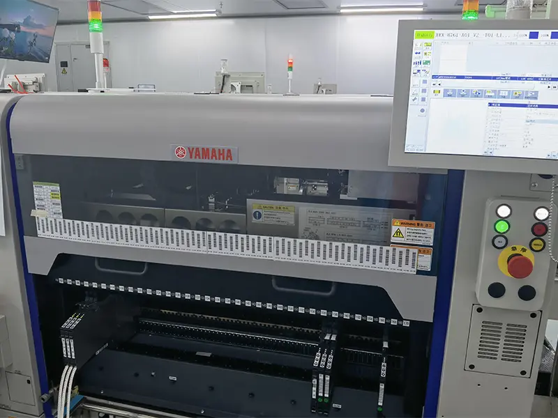
High-Speed YAMAHA Mounters
Equipped with dual-lane, high-speed multi-head placement modules capable of placing up to 45,000 components per hour per line, maintaining pinpoint accuracy on 01005 resistors and dense BGA arrays.
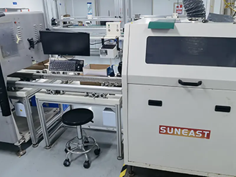
Pre-Reflow & Post-Reflow AOI
Pre-reflow optical validation catches component skew, tombstoning, and polarity rotation before soldering. Post-reflow 3D AOI uses multi-frequency moiré projection to verify perfect solder meniscus formation.
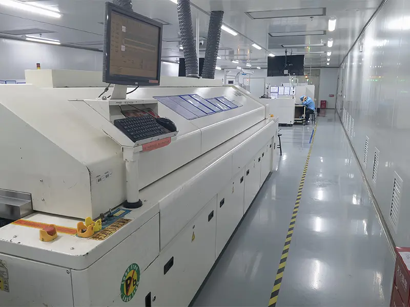
10-Zone Nitrogen Reflow Ovens
Computerized 10-zone reflow ovens running dynamic thermal profiles calibrated per assembly mass. Full nitrogen inerting guarantees zero oxidation, ideal wetting, and compliant RoHS lead-free soldering joints.

Automated SMT Flow
Cleanroom workshops with controlled electrostatic discharge (ESD) flooring, positive pressure filtration, and humidity regulation to ensure electronic semiconductor integrity across all shifts.
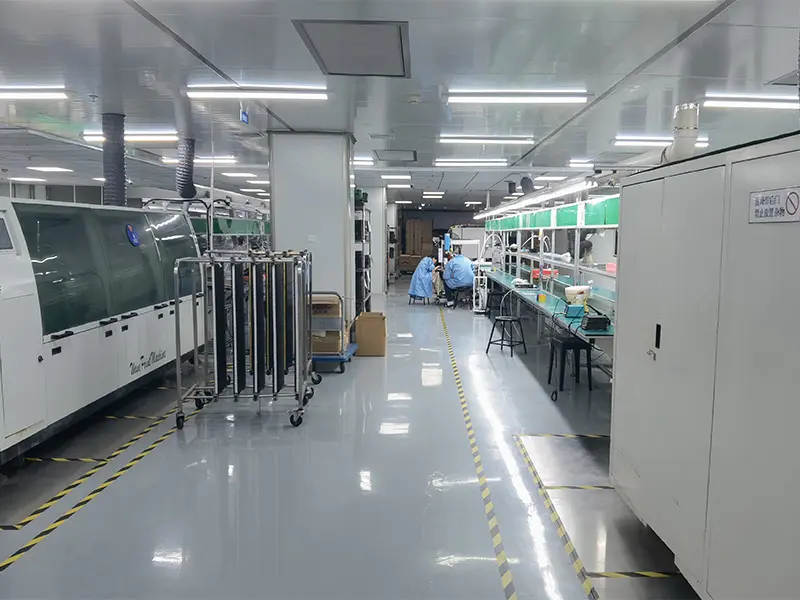
4-Line DIP & Selective Wave Solder
Through-hole insertion lines outfitted with automated dual-wave soldering and custom selective soldering fixtures to protect sensitive SMT components while achieving 100% pin barrel fill.
Global Sourcing Trends & Supply Chain Resilience for Hardware OEMs
In the wake of unprecedented geopolitical and supply chain shifts, the electronics hardware manufacturing landscape is undergoing a systemic structural transformation. Global original equipment manufacturers (OEMs) and high-growth technology ventures can no longer rely on single-channel component procurement or fragmented subcontractor handoffs. Leading technology organizations are transitioning toward agile turnkey electronic manufacturing partnerships that provide end-to-end transparency, robust risk diversification, and localized component leverage.
1. Direct BOM Scrubbing & Component Lifecycle Management
One of the most persistent bottlenecks in modern electronics commercialization is designing prototypes around components that are "Not Recommended for New Designs" (NRND) or approaching "End-of-Life" (EOL) status. When overseas engineers generate their Bill of Materials using catalog sites, they frequently select readily available single-quantity parts that carry 40-week lead times once volume ramps up. Our specialized DFM (Design for Manufacturability) and FMEA (Failure Mode and Effects Analysis) engineering review scrub every BOM line by line, evaluating lifecycle status, authorized distributors, and alternative pin-compatible drop-in parts before raw silicon orders are committed.
2. Defeating Counterfeit Risks via Franchised Pipeline Integrity
Component authenticity is paramount. The proliferation of substandard or reclaimed microchips in the open broker market presents catastrophic reliability risks for automotive, aerospace, and medical hardware. PCB ADEPT enforces an unbending incoming component pedigree. We source exclusively from authorized franchised distributors, original semiconductor foundries (TI, ADI, ST, Microchip, Infineon, NXP), or directly via automated DigiKey / Mouser procurement APIs. Every reel undergoes barcode verification, lot traceability indexing in our MES database, and destructive decapsulation or X-ray inspection when independent testing is mandated.
3. Green Electronics & ESG Manufacturing Governance
European and American regulatory bodies continue to tighten environmental compliance mandates (RoHS 3, REACH, WEEE, Conflict Minerals, halogen-free directives). Our automated SMT lines operate using lead-free SAC305 (Sn96.5/Ag3.0/Cu0.5) solder alloys, deionized closed-loop water cleaning systems, and energy-efficient nitrogen reflow systems, ensuring that your assembled PCBA is fully compliant with target export jurisdictions across the globe.
Accelerate Your DigiKey BOM to Finished PCBA
Send our senior engineering team your Gerber files (ODB++) and complete Bill of Materials today. Receive an exhaustive DFM analysis, component pricing cross-check, and turnkey manufacturing quote within 24 hours.
Frequently Asked Questions on DigiKey PCB Assembly
Clear, definitive technical answers to the most common questions international procurement teams and hardware engineers ask before contracting their builds.
Can PCB ADEPT assemble printed circuit boards using an exact DigiKey Bill of Materials (BOM)?
Yes, absolutely. Our quoting and component management software is natively integrated with DigiKey and Mouser catalog databases. You can simply upload your BOM containing DigiKey part numbers (DKPN), manufacturer part numbers (MPN), descriptions, and reference designators. Our engineering team will directly purchase the identical parts specified. Furthermore, we can flag parts that carry high premiums on catalog websites and suggest 100% pin-compatible, electrically identical alternatives from authorized domestic distributors to drastically reduce your BOM expense without compromising circuit integrity.
Do you support partial component consignment (kitted assembly) if we prefer to supply proprietary chips?
Yes. We offer fully customizable engagement models: Full Turnkey (we fabricate bare boards, source 100% of parts, and assemble), Partial Turnkey / Consignment (you drop-ship pre-programmed microcontrollers, security chips, or custom ASICs from your facility or DigiKey directly to our Shenzhen dock, and we source all standard passives, connectors, and bare PCBs), and Consigned Assembly (you provide all parts, and we provide precision SMT/THT assembly and testing).
What are your standard turnaround lead times for prototype PCBA vs. production volumes?
For rapid engineering prototypes (1 to 500 pcs), our typical turnaround ranges from 3 to 9 working days once component kitting is completed and Gerber engineering queries are resolved. For repeat or mid-to-high volume production batches, standard lead times are typically 15 to 25 business days, inclusive of bare board fabrication, complete automated SMT/DIP lines, post-assembly automated optical inspection (3D AOI), X-ray testing, and burn-in testing.
How do you guarantee the authenticity and quality of electronic components sourced in China?
Quality reliability and anti-counterfeiting are central pillars of our ISO 9001 quality system. We source exclusively through verified primary channels: authorized factory franchised distributors, original component manufacturers (such as TI, ST, ADI, NXP, Microchip, Murata), or directly via reputable international catalog houses (DigiKey, Mouser, Arrow). Every incoming reel passes through our Incoming Quality Control (IQC) laboratory, where we verify manufacturer packaging, date codes, moisture barrier bags, pin oxidation, and mark permanence. Critical active silicon components are logged in our MES system for full pedigree traceability down to the specific circuit board serial number.
What files are required to initiate an immediate DFM review and quotation?
To provide an accurate quote and free DFM report within 24 hours, please provide:
1. PCB Gerber Files: RS-274X or ODB++ format including all copper layers, solder mask, silkscreen, drill files, and board outline.
2. Bill of Materials (BOM): In Excel (.xls/.xlsx) or .csv format, detailing Reference Designators, Manufacturer Part Numbers (MPN) or DigiKey Part Numbers, Package/Footprint, and Quantity.
3. Pick-and-Place (Centroid / XY Data): Detailing component coordinates and rotation angle for automated SMT feeder setup.
4. Assembly Drawings / Testing Instructions: (Optional but recommended) Special requirements such as conformal coating zones, firmware flashing binaries, or custom functional testing steps.
Can you assemble ultra-fine pitch components such as 01005 passives and 0.3mm micro-BGAs?
Yes. Our automated SMT lines are fitted with advanced YAMAHA and Panasonic pick-and-place equipment capable of reliable placement down to 01005 (0402 metric) passives and fine-pitch BGAs with 0.30mm ball pitch. Solder paste deposition is strictly monitored with 3D Solder Paste Inspection (SPI) to prevent bridging or insufficient volume. All micro-BGAs, QFNs, and leadless ICs pass through our high-resolution 2D/3D X-Ray inspection equipment to ensure less than 5% solder voiding in compliance with IPC-A-610 Class 3 standards.
How does PCB ADEPT protect client intellectual property (IP) and design firmware?
We treat intellectual property with ironclad confidentiality. Prior to exchanging design files, we routinely execute formal, legally binding Non-Disclosure Agreements (NDAs). Design databases and Gerber archives are stored on access-restricted enterprise servers with air-gapped firewalls. Firmware programming is conducted in dedicated programming suites utilizing checksum-encrypted flashing jigs, and all client binaries are permanently scrubbed from flashing stations upon completion of the production order.
Do you provide full box build, custom enclosures, and final product packaging?
Yes, we are a comprehensive electronic manufacturing service (EMS) provider. In addition to high-density PCBA, our facility provides complete electromechanical box build assembly: custom injection-molded plastic housings, precision CNC aluminum enclosures, sheet metal fabrication, membrane switches, display integration, silicone potting, custom cable harness routing, final device burn-in testing, and retail-ready custom packaging designed for immediate distribution to consumer or industrial end users.
Specialized & High-Current Circuit Assemblies
Explore our extended electronics manufacturing capabilities: from IoT expansion boards to extreme heavy copper power distribution systems.

OEM Raspberry Pi HAT Mini Single-Board Computer
Turnkey customized daughterboard modules designed for IoT automation, smart telemetry, and embedded DIY computing with 40-pin GPIO pin header integration.
View Specifications
ODM Raspberry Pi HAT & Carrier Boards
Full-stack hardware engineering from schematic layout to SMT loading, integrating LoRa, Zigbee, CAN-bus, and cellular modems for commercial edge nodes.
View Specifications
Flexible PCB (FPC) Lightweight Bendable Circuitry
Ultra-thin polyimide substrates with high flexural endurance, ideal for dynamic hinges, wearable medical monitors, and compact consumer electronics.
View Specifications
Heavy Copper PCB (3oz–12oz) High Thermal Dissipation
Built for EV charging stations, power supplies, and solar inverters. Massive copper cross-sections providing superior heat transfer and immense current capacity.
View Specifications
High-Density Interconnect (HDI) Circuit Solutions
1+N+1 to Any-Layer HDI technology. Multi-lamination cycles with copper-filled microvias in pad (VIPPO), engineered for ultra-compact high-speed computing.
View Specifications
High Frequency PCBs for Low Signal Loss & Crosstalk
Fabricated on Rogers RO4003C/RO4350B laminates with strict dielectric thickness control (±5%) and controlled trace impedance (±7%) up to 77 GHz radar bands.
View Specifications
Multi-Layer Rigid-Flex Board Assembly & Fabrication
Eliminate fragile external ribbon connectors with durable integrated rigid-flex boards. Custom stiffeners, air-gap flex arm designs, and gold wire-bondable finishes.
View Specifications
ODM High Frequency & Hybrid Multilayer PCBs
Hybrid stack-up pressing (FR-4 + Rogers core) engineered to dramatically reduce raw board costs while maintaining gigahertz RF trace performance on top signal layers.
View SpecificationsAbout Shenzhen ICSLOVE Technology Co., Ltd. (PCB ADEPT)
Founded in Shenzhen—China's Silicon Valley and global hardware capital—Shenzhen ICSLOVE Technology Co., Ltd. (operating internationally under the brand PCB ADEPT) operates an 8,000 square meter advanced electronics manufacturing complex located at 5th Floor, Area B, Building 3, Anda Electronic Industrial Zone, Fuhai Subdistrict, Bao'an District, Shenzhen, China.
Our core technical leadership team brings over 15 years of deep electronic manufacturing services (EMS) engineering pedigree. Supported by 6 high-precision SMT lines, 4 automated DIP through-hole assembly lines, and a dedicated team of component procurement specialists, we have manufactured and shipped over 5,000 unique PCBA designs to customers across more than 50 countries worldwide. Whether your team is designing on DigiKey platforms for quick-turn prototype evaluation or ramping to high-volume commercial production, PCB ADEPT delivers uncompromised quality, unmatched agility, and significant cost advantages under a unified ISO 9001 quality framework.