
High-Quality China Suppliers for Single and Double-Sided Rigid Flex PCBs | Multi-Layer Rigid Flex PCB Factory Manufacturer, Suppliers
Product Description
What is Rigid Flex PCB?
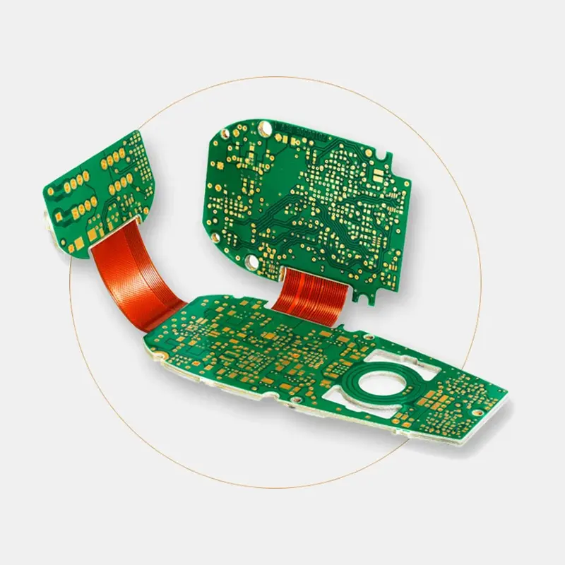
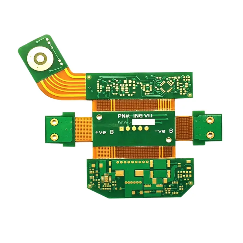
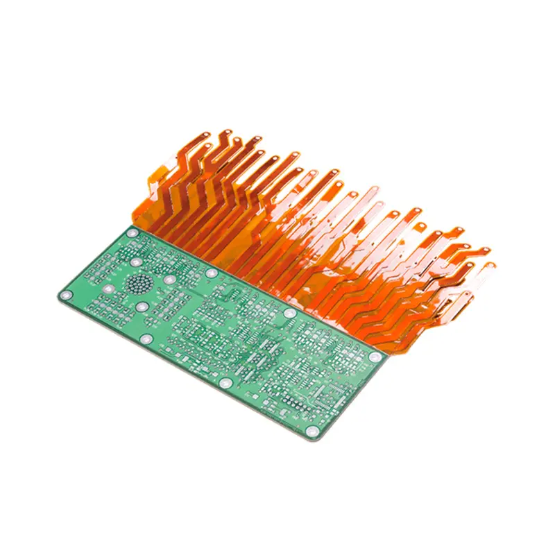
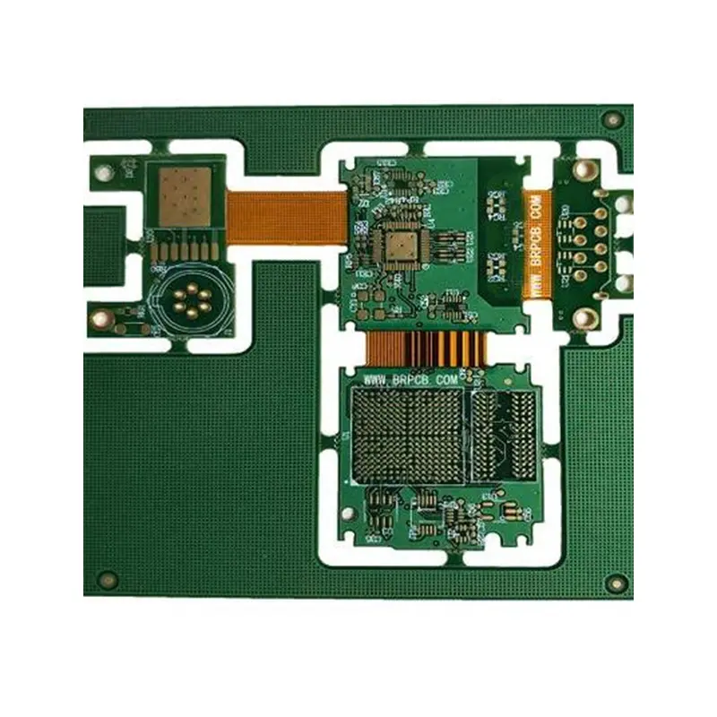
Rigid-Flex PCB (Rigid-Flex Printed Circuit Board) is a hybrid circuit board that combines the characteristics of rigid PCBs and flexible PCBs (flex PCBs) into a single integrated structure. It integrates rigid sections (for stable mounting of components) and flexible sections (for bending, folding, or dynamic movement) without the need for additional connectors, making it widely used in electronic devices that require compact design, reliability, and space optimization.
Core Components & Structure
A typical rigid-flex PCB consists of three key parts, layered and bonded together through specialized processes:
- 🔩 Rigid Sections: Made of traditional rigid substrate materials (e.g., FR-4, a glass-reinforced epoxy resin). These parts provide mechanical stability to support electronic components (such as chips, resistors, capacitors) and ensure structural integrity.
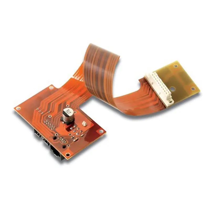
- 🌀 Flexible Sections: Composed of flexible substrates (common materials include polyimide, PI, or polyester, PET). These parts are thin, lightweight, and can be repeatedly bent, folded, or twisted, allowing the board to adapt to irregular shapes or dynamic environments.
- 🔗 Interconnect Layers: The rigid and flexible sections share internal conductive copper layers (signal traces, power lines, ground planes) that are seamlessly connected. This eliminates the need for wires, connectors, or solder joints between separate rigid and flex boards, reducing failure risks.
Key Advantages
- 📦 Space & Weight Savings: They can be folded to fit into tight, complex enclosures (e.g., foldable phones, wearables), reducing the overall size and weight of electronic devices.
- 🛡️ Enhanced Reliability: Fewer connectors and solder joints mean fewer potential points of failure (e.g., loose connections from vibration or aging), which is critical for high-reliability applications like aerospace equipment.
- ⚙️ Simplified Assembly: Integrating multiple rigid and flex parts into one board streamlines the manufacturing process, reducing assembly time and human error.
- 📡 Improved Performance: Continuous copper traces minimize signal loss and electromagnetic interference (EMI), ensuring stable signal transmission — essential for high-frequency devices.
Common Applications
- 📱 Consumer Electronics: Foldable smartphones, smartwatches, laptops, cameras, and earbuds (e.g., the hinge area of foldable phones uses flexible sections to connect rigid display and battery boards).
- 🚀 Aerospace & Defense: Satellites, aircraft avionics, and military equipment (they withstand extreme temperatures, vibration, and space constraints).
- 🚗 Automotive: In-vehicle infotainment systems, sensor modules, and advanced driver-assistance systems (ADAS) (adapt to the curved or confined spaces of car interiors).
- 🏥 Medical Devices: Portable monitors, implantable devices (e.g., pacemakers), and diagnostic equipment (offer biocompatibility, miniaturization, and durability).
The Types of Rigid Flex PCB
The classification dimensions of Rigid-Flex PCB are numerous. The core classification can be based on structural form, flexible area characteristics, number of layers, and adaptability to application scenarios. Different categories correspond to different process difficulties and usage requirements.
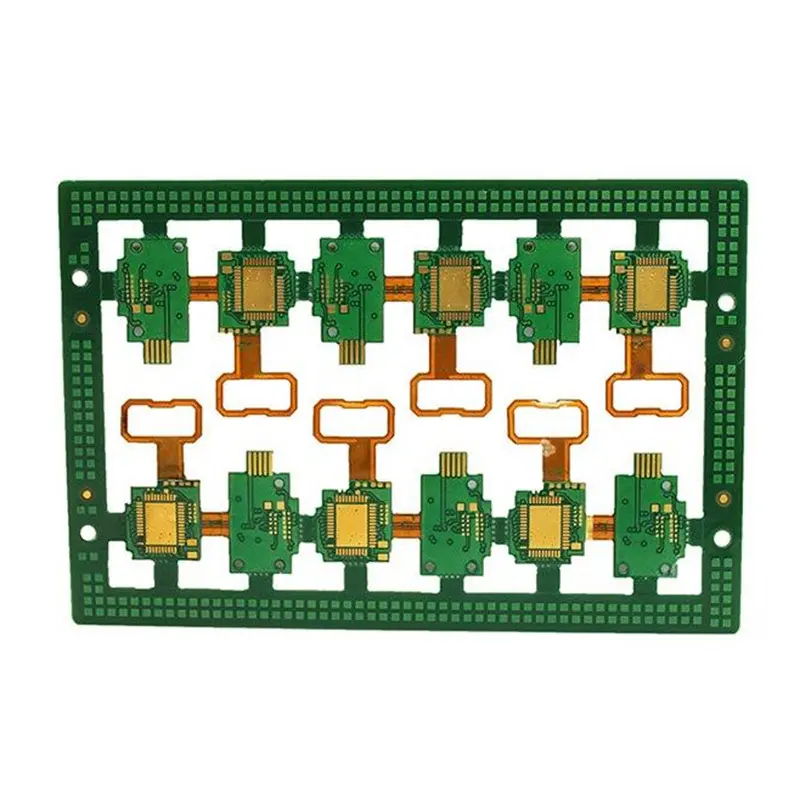
- Single Flexible Zone Rigid-Flex PCB: The entire board has only one continuous flexible zone, with both ends or one end connected to the rigid board. Simple structure, low cost — the most common basic model in consumer electronics such as laptop flat cables and headphone circuit boards.
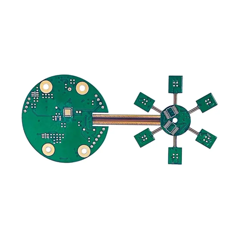
- Multi-Flexible Zone Rigid-Flex PCB: Contains two or more independent flexible zones, forming a complex structure through the series connection of multiple rigid boards. Suitable for industrial sensor modules and multi-camera lens module circuit boards.
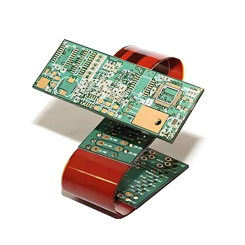
- Three-Dimensional Rigid-Flex PCB: The flexible area achieves bending and twisting in three-dimensional space, with rigid areas distributed in different spatial planes. Used in UAV fuselage control boards and car instrument panel integrated circuit boards.
- Static Rigid-Flex PCB: The flexible area is bent and shaped only once during assembly and maintains a fixed form during subsequent use. Core requirement is structural stability after shaping (e.g., foldable phone frames).
- Dynamic Rigid-Flex PCB: The flexible area withstands long-term repeated bending and twisting, requiring extremely high fatigue resistance. Typical applications include printer paper feed mechanism boards and wearable device opening/closing components.
- Single-Layer Rigid-Flex PCB: Contains only one layer of conductive copper foil. Simplest structure, lowest cost, suitable for low-complexity circuits such as simple toy control boards and small remote controls.
- Double-Layer Rigid-Flex PCB: Two layers of conductive copper foil with interlayer conduction achieved through vias. Widely used as peripheral modules for smartphones and tablet computers.
- Multi-Layer Rigid-Flex PCB (≥4 layers): Composed of alternating "rigid layer – flexible layer – rigid layer" superposition. High integration, suitable for aerospace satellite circuit boards and medical precision detection mainboards.
- High-Frequency Rigid-Flex PCB: Adopts flexible substrates with low dielectric constant and low loss (e.g., PTFE-modified polyimide). Suitable for 5G equipment, radar systems, and satellite communication equipment.
- High-Temperature Resistant Rigid-Flex PCB: Made of high-temperature resistant materials (e.g., special PI), operating stably within -55°C to 200°C. Used in aero engine peripheral equipment and industrial high-temperature sensors.
- HDI Rigid-Flex PCB: Uses micro-vias and fine line width/spacing technologies to enhance line density. Suitable for miniaturized devices such as smartwatches and implantable medical devices.
How to Design Rigid Flex PCB?
The design and production of rigid-flex PCBs need to take into account both the structural stability of rigid PCBs and the bending adaptability of flexible PCBs. During the design stage, potential risks in subsequent production and use should be avoided. Below are the detailed design key points.
- Clear Zone Boundaries: A transition zone (usually 0.5–1mm) should be reserved at the boundary between the rigid zone and the flexible zone to prevent components, vias, and copper foils from crossing the boundary. The edges of the flexible zone need to be rounded (radius ≥1mm) to reduce stress concentration.
- Flexible Zone Bending Planning: The minimum bending radius of the inner copper foil should be ≥10× the thickness of the flexible substrate; outer copper foil ≥15×. Avoid overlapping and bending in the flexible zone to prevent long-term compression from damaging the circuit.
- Component Layout: Heat-generating components should be concentrated in the rigid area and far away from the flexible area. Heavy-duty components need to be fixed in rigid areas with reserved heat dissipation space and fixing holes.
- Line Direction: In the flexible zone, prefer horizontal line direction (parallel to the bending direction) to reduce tensile/compressive damage to the copper foil. Minimum line width/spacing recommended ≥0.1mm.
- Stacking Structure: For multi-layer boards, the flexible layer should adopt a symmetrical structure to prevent warping. Rigid core materials are prohibited in the flexible zone; adhesive should be flexible materials such as acrylic.
- Via and Grounding: Metallized vias are prohibited in the flexible zone. All vias must remain in the rigid zone and be at least 1mm away from the flexible zone boundary. In high-frequency scenarios, "microstrip line" or "ribbon line" structures can optimize signal transmission.
- Flexible Substrate: For dynamic bending, choose polyimide (PI) with good fatigue resistance. For static scenarios, polyester (PET) with lower cost can be selected. High-frequency equipment should use PI substrates with low dielectric constants (e.g., PTFE-modified PI).
- Copper Foil & Covering Film: For flexible areas, rolled copper foil (with good ductility and bending resistance) is preferred. The surface of the flexible zone should be covered with a flexible PI covering film, with edges extending 0.2–0.3mm beyond the copper foil for protection and insulation.

Key Points of Manufacturing
Substrate cleaning: The surface of the flexible PI substrate is prone to adsorbing impurities. Remove oil stains and oxide layers through plasma cleaning or chemical treatment to enhance copper foil adhesion. Rigid FR-4 substrates need to be dried and dehumidified to prevent air bubbles during lamination.
Precise lamination: Temperature, pressure, and time need to be controlled. Bonding parameters of the flexible and rigid zones should be set differently. The stepwise lamination method is adopted — first laminating the flexible layer, then laminating with the rigid layer to ensure tight interlayer bonding.
High-precision exposure: Flexible substrates are prone to stretching. Special fixtures should be used for fixation during exposure. Ultraviolet parallel light exposure machines are adopted to control line width error in the flexible zone within ±0.02mm.
Etching process optimization: Alkaline etching solution is used to treat the copper foil in the flexible zone. The etching speed is slightly lower than that in the rigid zone to prevent excessive etching causing line breakage. After etching, clean promptly to avoid residual liquid corrosion.
Flexible zone contour cutting: Processed by laser cutting (CO₂ laser or ultraviolet laser) with smooth cuts and no burrs, avoiding tearing of the base material caused by mechanical cutting.
Rigid zone forming: Formed by CNC milling with edges deburred and chamfered. The boundary between rigid and flexible zones needs to be ground a second time to ensure a smooth transition and reduce stress concentration during bending.
Surface treatment: Rigid areas can undergo tin spraying, gold plating, and OSP surface treatments to enhance soldering performance. High-temperature treatments such as tin spraying are prohibited on flexible zone surfaces to prevent base material deformation.
Full-process inspection: Interlayer adhesion (peel test) and line conductivity (flying probe test) are inspected during production. Finished products undergo bending tests (dynamic bending simulates tens of thousands of cycles) and high/low temperature environment tests.
| Category | Parameter | Standard | Advanced |
|---|---|---|---|
| RIGID FLEX PCB | Flex Layers | Lamination structure ≤4L; Book structure ≤10L | Lamination structure ≤4L; Book structure ≤12L |
| Max. Panel Size (shipping) | 210MM × 480MM | 460MM × 480MM | |
| FPC Dielectric Thickness | 2MIL, 3MIL, 4MIL | 1MIL | |
| PTH Rigid-Flex Transition Area | ≤1.2MM | ≤1.0MM | |
| Pattern Spacing, Rigid Area to Rigid-Flex Transition Area | ≥1.2MM | ≥0.9MM | |
| RIGID FLEX PCB | Rigid-Flex Structure | Typical structure, Flying tail structure, Multi-flex book structure, Two-flex lamination structure, Single-sided asymmetric structure, Asymmetric structure, etc. | |









