
OEM High Frequency PCB Suppliers in China | Factory Solutions for Signal Loss, Crosstalk, and EMI Issues Suppliers, Factories
Product Description
What is High Frequency PCB?
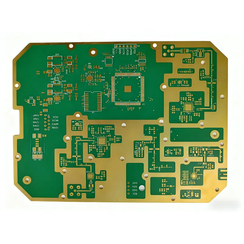
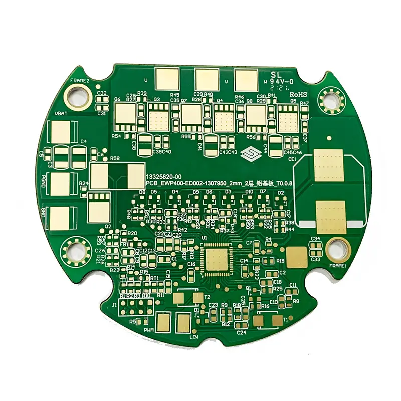
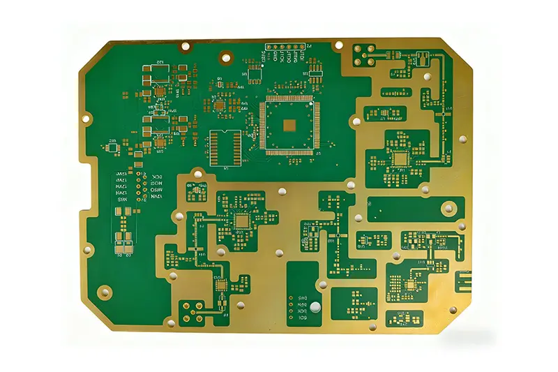
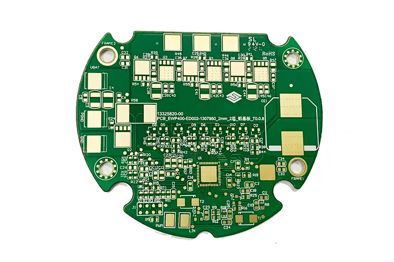
High-frequency PCBs are special printed circuit boards specifically designed to handle high-frequency signals (typically referring to frequencies above 500MHz or digital signal rise times less than 1 nanosecond).
Main Application Fields
Core Material Selection Principles
High-frequency signals are easily affected by the dielectric properties and losses of the substrate. Material selection is the core of high-frequency PCBs.
| Material Type | Key Parameters | Recommended Material/Specification | Applicable Scene |
|---|---|---|---|
| Base material |
Dielectric constant (Dk) Dielectric loss tangent of Angle (Df) Coefficient of thermal expansion (CTE) |
High-frequency dedicated substrate - PTFE (polytetrafluoroethylene, Dk=2.1-2.6, Df≤0.0009) - Rogers series (such as RO4350B, Dk=3.48, Df=0.0037) - Modified epoxy resin (FR-4 high-frequency version, Dk=3.8-4.2, Df≤0.01) |
PTFE/Rogers: Millimeter wave, radar, 5G base station High-frequency FR-4: Consumer Electronics (Mobile phones, routers) |
| Copper foil | Surface roughness | Low profile copper foil (LP)/very low profile copper foil (VLP), roughness ≤1.0μm | Reduce the transmission loss of signals on the surface of copper foil (skin effect) |
| Solder mask layer | Dielectric loss | High-frequency special solder mask oil (Df≤0.01) | Avoid increasing signal attenuation by the solder mask layer |
Key Design Points
- The core of high-frequency PCBs needs to control the characteristic impedance (such as 50Ω single-ended impedance, 100Ω differential impedance), with the deviation being ≤±5% (±10% for ordinary PCBs).
- Impedance calculation: It is necessary to combine the base material Dk, plate thickness, line width/line spacing, and copper foil thickness. It can be simulated through professional software (such as Polar SI9000).
- Example: RO4350B substrate (thickness 0.254mm), with a single-ended impedance of 50Ω corresponding to a line width of approximately 0.8mm.
- Impedance compensation: Considering the influence of etching side etching and solder mask coverage, a compensation amount of ±0.02mm should be reserved for the line width.
- Reduce transmission loss: The traces should be as short and straight as possible, avoiding right angles or acute angles (which are prone to reflection at high frequencies), and the radius of the fillet should be no less than 0.5mm.
- Differential traces: Should be of equal length and spacing (length difference ≤5mil), and ground wrapping treatment should be carried out (the distance between the ground wire and the differential wire should be ≤2 times the line width) to reduce EMI interference.
- Skin effect response: High-frequency current is concentrated on the surface of the copper foil. Silver-plated copper foil can be used (to reduce surface resistance), or the traces can be widened (to reduce current density).
- Complete ground layer: High-frequency PCBs need to be designed with a complete ground Plane (GND Plane) to avoid ground layer segmentation and reduce the length of the signal return path. The distance between the ground layer and the signal layer should be no more than 0.2mm to enhance coupling and reduce impedance.
- Shielding measures: For sensitive high-frequency areas (such as RF chips), metal shielding covers can be designed. The grounding of the shielding cover must be reliable (multiple grounding points, spacing ≤λ/20, where λ is the signal wavelength).
- Heat dissipation: High-frequency devices (such as power amplifiers) generate a large amount of heat, so heat dissipation pads and metallized via arrays (via diameter ≥0.3mm, spacing ≤1mm) need to be designed to enhance heat dissipation.
- Device packaging: Prioritize miniaturized and low-parasitic parameter packaging (such as QFN, LGA) to reduce signal reflection introduced by the packaging.
Manufacturing Process Control
- Line width/line spacing tolerance: ≤±0.01mm (±0.02mm for ordinary PCBs), using high-precision laser direct imaging (LDI) technology to replace traditional film exposure.
- Lamination accuracy: Interlayer alignment deviation ≤0.02mm, avoiding impedance offset; The bonding temperature and pressure need to match the characteristics of the base material (for example, PTFE base materials require high-temperature and high-pressure bonding).
- Etching process: Micro-etching technology is adopted to reduce the surface roughness of the copper foil and avoid increasing transmission loss. The lateral erosion is ≤0.01mm.
- Surface treatment: Electroless nickel gold plating (ENIG) or silver plating is preferred to avoid OSP (organic film increases contact resistance). The thickness of the gold layer should be ≤0.1μm. If it is too thick, it will easily increase the loss.
The core of high-frequency PCBs lies in "reducing signal loss, ensuring precise impedance, and minimizing electromagnetic interference". It requires full-process control from "low-loss substrate selection → precise impedance design → high-precision manufacturing". For different high-frequency scenarios (such as 1GHz vs 60GHz), the substrate and process parameters need to be adjusted specifically.
Send Inquiry
Frequently Asked Questions
What is a High-Frequency PCB?
High-frequency PCBs are specialized printed circuit boards designed to transmit signals above 500MHz or handle digital signal rise times of less than 1 nanosecond with minimal signal loss.
What are the primary applications of High-Frequency PCBs?
They are critical in communication infrastructure (5G/6G base stations), automotive electronics (radar and ADAS), aerospace/defense systems, high-speed computing (servers, switches), and precise test and measurement instruments.
How is impedance controlled in High-Frequency PCBs?
Impedance is strictly controlled within a deviation of ≤±5% (compared to ±10% in standard boards). This is achieved by precise calculations of dielectric constant (Dk), board thickness, trace width, spacing, and copper thickness, often simulated using tools like Polar SI9000.
Which materials are recommended for High-Frequency PCB substrates?
Common materials include PTFE (Teflon) for its extremely low dielectric loss (Df ≤ 0.0009), Rogers series (e.g., RO4350B), and high-frequency modified epoxy resins (FR-4 high-frequency versions) depending on the performance requirements and cost limits.
What is the significance of copper foil roughness in HF boards?
Due to the skin effect, high-frequency current travels primarily along the outer surface of the copper. Rougher surfaces increase signal path length and resistance. Using low profile (LP) or very low profile (VLP) copper foil (roughness ≤ 1.0μm) minimizes this transmission loss.
What manufacturing tolerances are required for High-Frequency PCBs?
High-frequency PCBs require a trace width/spacing tolerance of ≤±0.01mm, using Laser Direct Imaging (LDI) instead of traditional film. Interlayer lamination alignment deviation must be kept ≤0.02mm to avoid impedance shifts.









