
ODM Multilayer PCB Suppliers in China | 1-60 Layers Factory with IPC2 Quality and 48-Hour Lead Time Suppliers, Factories
Product Description
The core advantage of multilayer PCBs lies in their ability to implement complex wiring within limited space, meeting the miniaturization and high-performance requirements of electronic products. They are widely used in smartphones, servers, medical devices, and other fields.
In their structure:
- Conductive layers (copper foil) transmit signals and power;
- Insulating layers are mostly prepregs (e.g., epoxy resin);
- Solder mask layers protect circuits from short circuits;
- Surface finishing prevents copper foil oxidation.
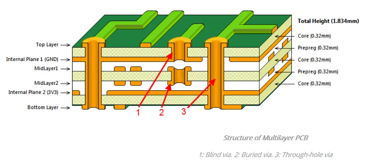
The diagram below shows the stackup structure of a 6-layer 1-step HDI (High-Density Interconnect) multilayer PCB, illustrating its layer stacking and via design:
| Design Challenge | Specific Issues | Solutions |
|---|---|---|
| Signal Integrity | High-speed signal transmission is prone to reflection and crosstalk, leading to signal distortion. The risk of crosstalk increases with more layers. |
• Adopt equal-length differential routing; maintain a spacing of at least 3× the line width for high-speed signals. • Add matching resistors (e.g., 50Ω) at the signal source. • Route high-speed signals in inner layers and isolate interference with ground planes. |
| Power Integrity | Power planes suffer from noise and voltage fluctuations; multiple voltage supplies are prone to mutual interference, causing chip crashes. |
• Arrange power layers adjacent to ground layers for filter capacitor coupling. • Place decoupling capacitors (e.g., 0.1μF) near chip pins. • Split power planes and isolate cross-split areas with beads. |
| Wiring and Routability | Increased layers result in limited wiring space; some circuits are difficult to route and may become disorganized. |
• Layout by functional partitions and concentrate associated components. • Route high-speed signals in inner layers and low-speed control signals in outer layers. • Reduce the width of non-critical signal lines to reserve routing channels. |
| Heat Dissipation | High-density layout causes heat accumulation in high-power components, damaging devices and affecting performance. |
• Drill 1–3mm thermal vias under heat-generating components. • Lay large-area thermal copper foil or install heat sinks. • Disperse high-power components and align with the device's air duct design. |
| Interlayer Alignment & Process Issues | More layers require more lamination cycles (e.g., an 8-layer board needs 7 laminations); copper foil offset between layers (exceeding 30μm may cause short circuits) and cracks during drilling are common. |
• Use advanced materials such as ultra-low profile copper foil. • Employ laser drilling equipment to control precision within ±15μm. • Adopt vacuum laminators to reduce pressure fluctuations during lamination. |
- Blind via
- HDI (High-Density Interconnect)
- Differential routing
- Decoupling capacitor
- Thermal via
- Vacuum laminator
The manufacturing process of multilayer PCBs is complex. Parameter deviations or improper operations in any link — from early material selection to final shaping and testing — may affect the quality of finished products. Below are the critical considerations for each core manufacturing stage:
Material Matching
- Choose substrates based on application scenarios: Cost-effective FR-4 substrates are suitable for general consumer electronics, while Rogers materials (low dielectric loss) or polyimide materials (high temperature resistance) are ideal for high-frequency communication devices or aerospace equipment.
- Select copper foil thickness according to current requirements: Thicker copper foil is recommended for high-current power circuits to reduce heat generation.
- Control the resin content of prepregs to avoid impacting interlayer adhesion and signal transmission.
Circuit Patterning and Surface Treatment
- After transferring circuit patterns to copper-clad laminates via exposure and development, precisely control etching parameters to prevent line width deviations or residual circuits.
- Conduct black oxidation or brown oxidation treatment on the board surface after etching to increase copper foil roughness, enhance interlayer bonding strength during subsequent lamination, and avoid delamination.
- This is a critical step to stack and bond inner layers, prepregs, and outer copper foils.
- Stack materials in strict accordance with the designed sequence to avoid interlayer misalignment.
- Strictly control lamination parameters: Temperature is typically maintained at 180–220℃, pressure at 3–5MPa, and lamination time must be precisely managed. Imbalanced parameters may cause defects such as bubbles or delamination in the board.
- Prioritize even-layer stacking with a symmetrical structure to minimize board warpage after lamination.
Precision Drilling
- Use CNC drilling machines to ensure hole position accuracy: The diameter of standard through-holes should be controlled above 0.2mm, with a tolerance of ±0.05mm or less.
- Distinguish application scenarios for through-holes, blind vias, and buried vias to avoid unnecessary complexity. For example, buried vias can be used for BGA packages but require proper hole plugging.
Hole Metallization Quality
- Form conductive hole walls through electroless copper plating and electrolytic copper plating; control plating thickness and uniformity. Insufficient or uneven plating may lead to voids or fractures in hole walls, affecting interlayer connectivity.
- Remove residual impurities from hole walls to prevent plating peeling.
Outer Circuit Processing
- The process is similar to inner layer fabrication, but higher precision is required as outer circuits directly affect component soldering and signal transmission.
- Ensure line width/spacing meets design requirements during photolithography, and avoid defects such as circuit burrs or short circuits.
Appropriate Surface Finish Selection
- HASL (Hot Air Solder Leveling): Cost-effective with good solderability, suitable for consumer electronics.
- Immersion Gold: Flat surface and stable performance, ideal for high-end precision equipment.
- OSP (Organic Solderability Preservative): Low-cost for mild operating environments, but note its poor protection under high temperature and humidity.
Precision Shaping
- Use CNC routing machines to process the board outline, with cutting precision controlled within ±0.2mm. For special structures such as V-cuts, control the cutting depth to avoid board fracture.
- Reserve 3–5mm wide process edges to facilitate subsequent SMT assembly and testing.
Comprehensive Inspection
- Conduct visual inspection with AOI (Automated Optical Inspection) equipment to detect defects such as open circuits or uneven solder mask.
- Perform electrical performance tests (e.g., flying probe test, ICT test) to ensure impedance deviation is within ±10%.
- Use X-ray inspection for hidden multilayer circuits to verify via quality and interlayer alignment, eliminating potential defects.
- Prepreg
- Black oxidation / Brown oxidation
- Delamination
- Blind via / Buried via
- Electroless copper plating / Electrolytic copper plating
- HASL (Hot Air Solder Leveling)
- Immersion Gold
- OSP (Organic Solderability Preservative)
- AOI (Automated Optical Inspection)
- Flying probe test / ICT (In-Circuit Test)
- Process edge









