
ODM China Suppliers of High-Quality Rigid Flex PCB: Single, Double-Sided, and Multi-Layer Factory Solutions Manufacturer, Supplier
Product Description
What is Rigid Flex PCB?
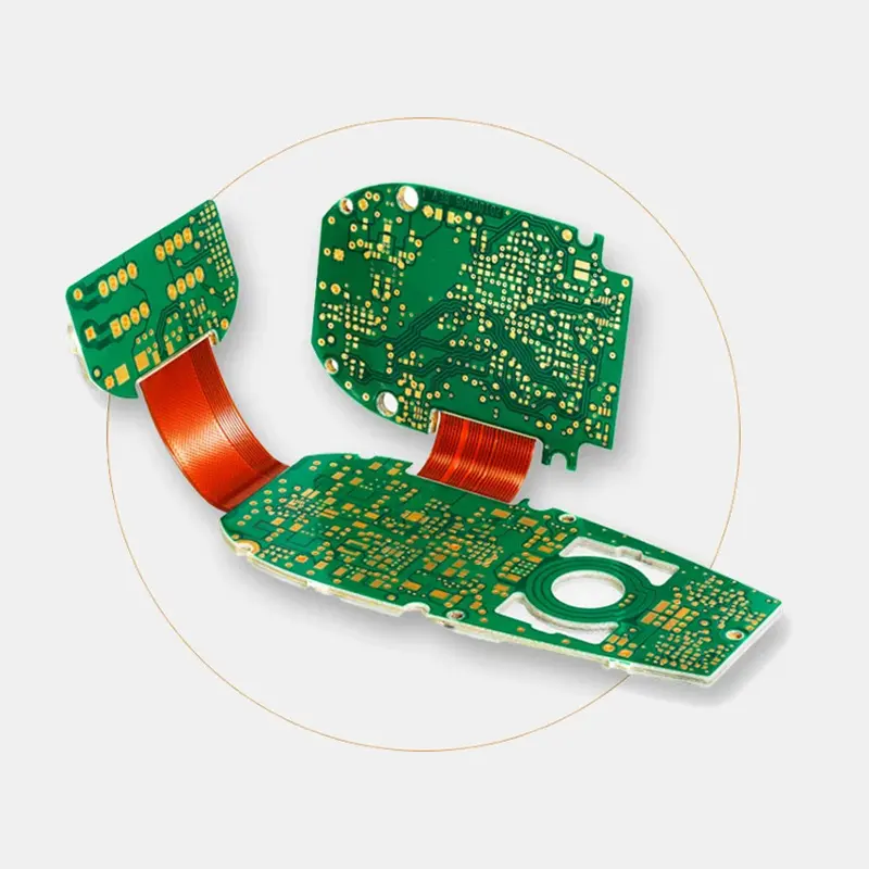
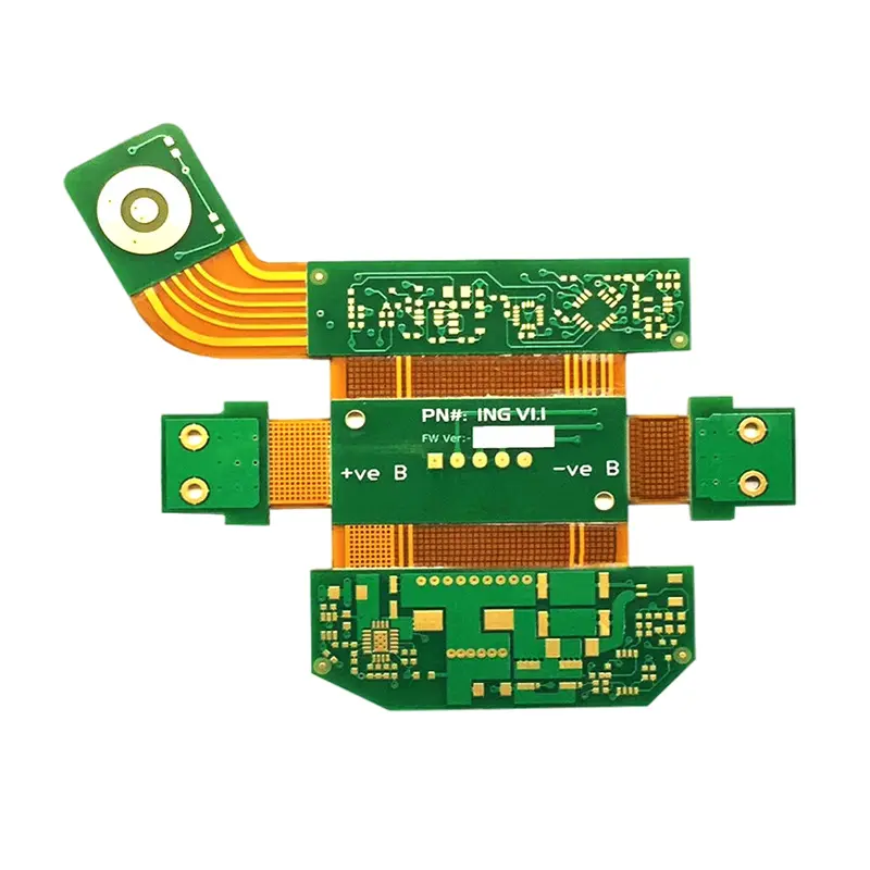
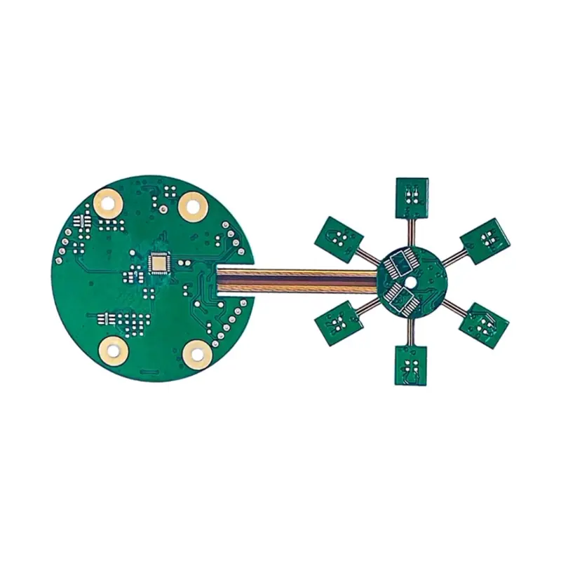
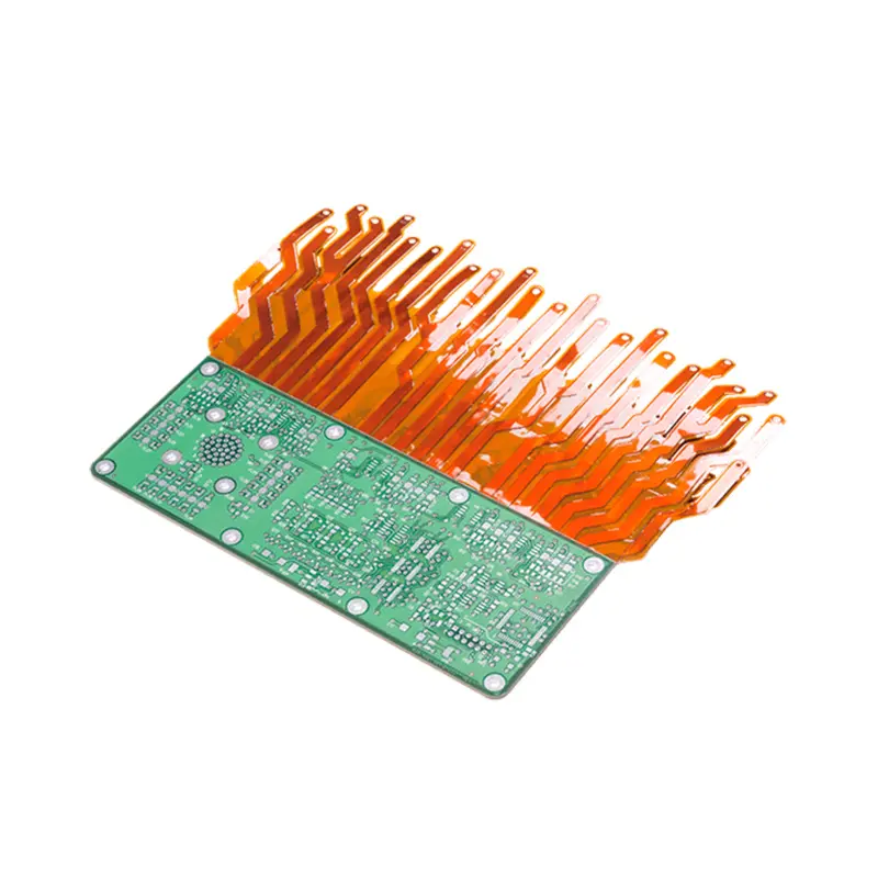
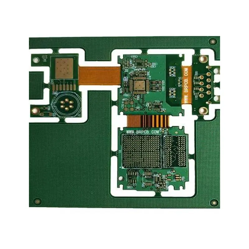
Rigid-Flex PCB (Rigid-Flex Printed Circuit Board) is a hybrid circuit board that combines the characteristics of rigid PCBs and flexible PCBs (flex PCBs) into a single integrated structure. It integrates rigid sections (for stable mounting of components) and flexible sections (for bending, folding, or dynamic movement) without the need for additional connectors, making it widely used in electronic devices that require compact design, reliability, and space optimization.
Core Components & Structure
A typical rigid-flex PCB consists of three key parts, layered and bonded together through specialized processes:
Made of traditional rigid substrate materials (e.g., FR-4, a glass-reinforced epoxy resin). These parts provide mechanical stability to support electronic components (such as chips, resistors, capacitors) and ensure structural integrity.
Composed of flexible substrates (common materials include polyimide, PI, or polyester, PET). These parts are thin, lightweight, and can be repeatedly bent, folded, or twisted, allowing the board to adapt to irregular shapes or dynamic environments.
The rigid and flexible sections share internal conductive copper layers (signal traces, power lines, ground planes) that are seamlessly connected. This eliminates the need for wires, connectors, or solder joints, significantly reducing failure risks.
Key Advantages
Compared to standalone rigid PCBs or flex PCBs, rigid-flex PCBs offer distinct benefits:
They can be folded to fit into tight, complex enclosures (e.g., foldable phones, wearables), reducing the overall size and weight of electronic devices.
Fewer connectors and solder joints mean fewer potential points of failure (e.g., loose connections from vibration or aging), which is critical for high-reliability applications.
Integrating multiple rigid and flex parts into one board streamlines the manufacturing process, reducing assembly time and human error.
Continuous copper traces minimize signal loss and electromagnetic interference (EMI), ensuring stable signal transmission—essential for high-frequency devices.
Common Applications
Rigid-flex PCBs are indispensable in industries where space, reliability, and flexibility are paramount:
- Consumer Electronics: Foldable smartphones, smartwatches, laptops, cameras, and earbuds (e.g., the hinge area of foldable phones uses flexible sections to connect rigid display and battery boards).
- Aerospace & Defense: Satellites, aircraft avionics, and military equipment (they withstand extreme temperatures, vibration, and space constraints).
- Automotive: In-vehicle infotainment systems, sensor modules, and advanced driver-assistance systems (ADAS) (adapt to the curved or confined spaces of car interiors).
- Medical Devices: Portable monitors, implantable devices (e.g., pacemakers), and diagnostic equipment (offer biocompatibility, miniaturization, and durability).
- Custom Solutions: Would you like me to elaborate on the manufacturing process of rigid-flex PCBs or the material selection criteria for different applications?
The Types of Rigid Flex PCB
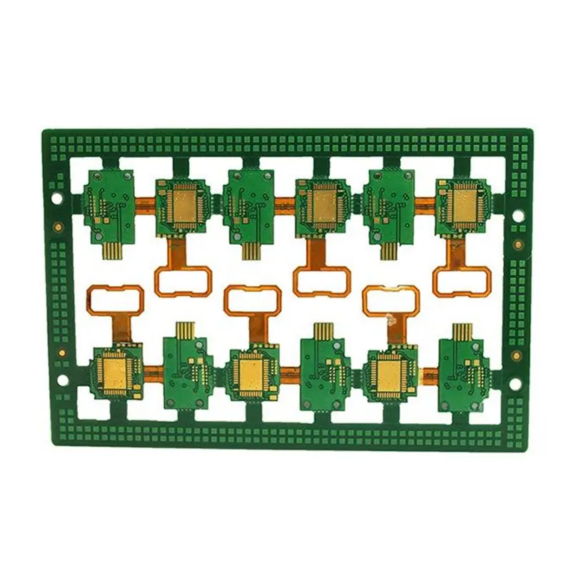
The classification dimensions of Rigid-Flex PCBs are numerous. Mainstream classifications are based on structural form, flexible area characteristics, layer counts, and specialized applications:
Classified by Structural Form
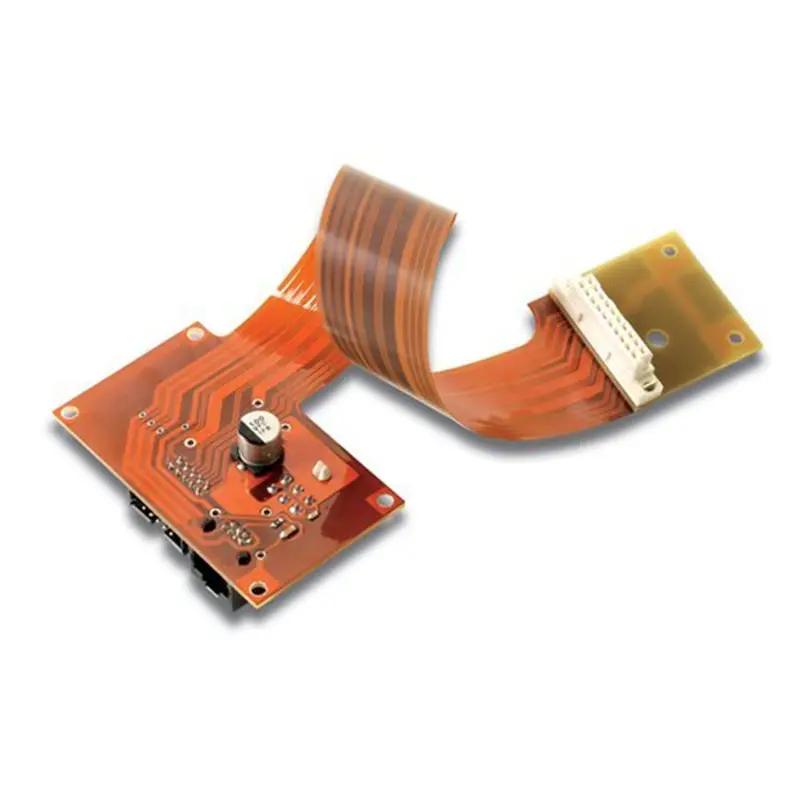
• Single Flexible Zone Rigid-Flex PCB: Features one continuous flexible zone connecting rigid boards at either or both ends. Ideal for folding or hinge mechanisms such as laptops or headphones; low cost and structural simplicity.
• Multi-Flexible Zone Rigid-Flex PCB: Contains two or more independent flexible zones linking multiple rigid sections in series. Suitable for multi-directional bending and distributed module placement like smartphone multi-camera modules.
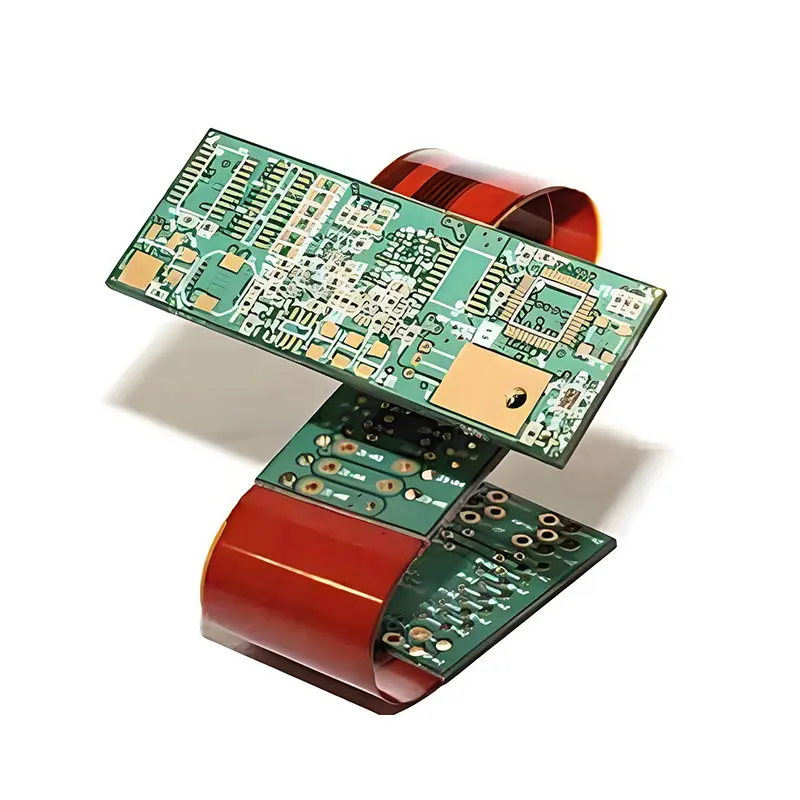
• Three-Dimensional Rigid-Flex PCB: Allows multi-planar spatial bending and twisting, connecting rigid areas distributed along 3D axes (e.g., UAV avionics and curved automotive dashboard controllers).
Classified by Characteristics of Flexible Regions
• Static Rigid-Flex PCB: Bent and shaped once during assembly, maintaining a fixed form throughout service (e.g., internal folding phone frame circuitry).
• Dynamic Rigid-Flex PCB: Designed to withstand continuous, repeated flexing cycles without failure (tens of thousands of bends), essential for printer feed heads and wearable hinges.
Classified by the Number of Circuit Layers
• Single-Layer: Uses one copper conductive layer across rigid and flex zones for basic, low-complexity circuits.
• Double-Layer: Employs two copper layers with plated via interconnects; commonly utilized in handheld smart device modules.
• Multi-Layer (≥4 Layers): Stacked with alternating rigid and flex cores, supporting complex power, ground, and signal routings for medical instruments and aerospace payloads.
Classified by Special Function Adaptation
• High-Frequency: Utilizes low-loss substrates (e.g., PTFE-modified PI) for minimal signal attenuation in 5G and radar systems.
• High-Temperature Resistant: Operates reliably from -55℃ to 200℃+ using high-grade PI matrices for automotive powertrains and aerospace engine bay sensors.
• High-Density Interconnect (HDI): Features micro-vias and ultra-fine line pitch for miniaturized footprints like pacemakers and smart wearables.
How to Design Rigid Flex PCB?
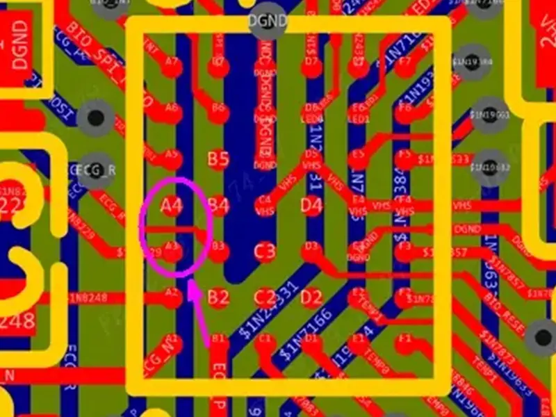
Design is central to the performance and reliability of rigid-flex boards. Key considerations include:
• Transition zones (0.5–1.0mm) reserved at the rigid-flex boundary without vias or traces crossing abruptly.
• Rounded flexible edges (radius ≥1mm) to mitigate stress concentration.
• Dynamic bending radius must meet: inner copper ≥10× substrate thickness; outer copper ≥15× thickness.
• High heat and heavy components placed securely in rigid areas only.
• Route traces perpendicular to the bend line in flexible zones; avoid sharp 90-degree corners.
• Minimum line width/spacing ≥0.1mm in flex regions.
• Balanced, symmetrical layer stackups prevent warpage.
• Metallized vias prohibited in flexible zones (must be ≥1mm away from transition line).
• Dynamic applications require high-ductility Polyimide (PI) and rolled annealed (RA) copper foil.
• Static assemblies can use cost-effective PET substrates and electro-deposited copper.
• Flexible coverlays (PI film) extend 0.2–0.3mm beyond copper boundaries for robust insulation.

Key Points of Manufacturing
Fabricating rigid-flex circuit boards involves combining rigid FR-4 and flexible polyimide workflows under strict precision parameters:
Plasma or chemical cleaning eliminates oxides on PI films to enhance copper adhesion. Stepwise lamination with differentiated pressure and temperature curves ensures void-free, delamination-resistant bonding between rigid and flexible layers.
Specialized tooling holds flexible layers flat during UV parallel-beam exposure. Alkaline etching with tightly controlled rates ensures flex zone line tolerances remain within ±0.02mm without undercutting.
UV or CO₂ laser cutting delivers burr-free flex contours and prevents micro-tearing. Rigid profiles are shaped via precision CNC milling, followed by edge secondary chamfering at transition zones.
Surface plating (ENIG, OSP, Immersion Tin) is restricted to rigid pads to prevent coverlay degradation. Comprehensive quality verification includes peel strength testing, flying probe electrical tests, thermal stress cycles, and multi-thousand dynamic bend simulations.
Rigid-Flexible PCB Capability Matrix
| Parameter / Capability Item | Standard Specification | Advanced Specification | |
|---|---|---|---|
| Rigid-Flex PCB | Flex Layers | Lamination structure ≤ 4L; Book structure ≤ 10L | Lamination structure ≤ 4L; Book structure ≤ 12L |
| Max. Panel Size (Shipping) | 210mm × 480mm | 460mm × 480mm | |
| FPC Dielectric Thickness | 2 mil, 3 mil, 4 mil | 1 mil | |
| PTH Rigid-Flex Transition Area | ≤ 1.2mm | ≤ 1.0mm | |
| Pattern Spacing (Rigid to Transition Area) | ≥ 1.2mm | ≥ 0.9mm | |
| Rigid-Flex Structure Types | Typical structure, Flying tail structure, Multi-flex book structure, Two-flex lamination structure, Single-sided asymmetric structure, Asymmetric structure, etc. | ||
Send Inquiry
Frequently Asked Questions (FAQ)
Q1 What is the primary advantage of a rigid-flex PCB over traditional wire harnesses?
Rigid-flex PCBs eliminate bulky wire harnesses and physical solder connectors, reducing package weight and volume by up to 60%, while removing common points of connection failure caused by shock and vibration.
Q2 What is the difference between static and dynamic rigid-flex PCBs?
Static (flex-to-install) boards are bent only once during product assembly and maintain their fixed 3D shape. Dynamic boards are engineered to endure tens of thousands of repeated folding cycles during normal product operation (e.g., foldable device hinges).
Q3 Which copper type is recommended for flexible circuit sections?
Rolled Annealed (RA) copper foil is preferred for flexible and dynamic zones due to its elongated grain structure that resists fatigue from bending. Electro-deposited (ED) copper is typically used for rigid zones.
Q4 Why are vias prohibited in the flexible zone of a rigid-flex board?
Plated through-holes (vias) create localized rigidity and high mechanical stress points. Placing them in bendable areas leads to trace cracking, barrel fracture, or delamination during flexing.
Q5 What standard design rules apply to the flexible bending radius?
For dynamic bending applications, the minimum bend radius must be at least 10 times the flexible circuit thickness for single/double-sided layers and at least 15 to 20 times the thickness for multi-layer flex configurations.
Q6 How do rigid-flex boards improve high-frequency signal integrity?
By routing unbroken copper conductors directly from rigid sections across flex zones without intervening connector interfaces, impedance discontinuities and signal reflection are minimized, ensuring clean high-speed transmission.









