
Famous High-Quality Multilayer PCB Suppliers in China - 1-60 Layers, IPC2 Grade, Fastest Lead Time 48 Hours Companies, Company
Product Description
A multilayer PCB (Printed Circuit Board) consists of three or more conductive layers (signal layers, power layers, ground layers, etc.) alternately stacked with insulating layers, bonded together under high temperature and pressure. It achieves electrical connection between different layers through structures such as through-holes and blind vias. Below is a detailed explanation of its definition, core design challenges, and corresponding solutions, supplemented by diagrams for better understanding.
The core advantage of multilayer PCBs lies in their ability to implement complex wiring within limited space, meeting the miniaturization and high-performance requirements of electronic products. They are widely used in smartphones, servers, medical devices, and other fields.
In their structure:
- Conductive layers (copper foil): Transmit signals and power;
- Insulating layers: Are mostly prepregs (e.g., epoxy resin);
- Solder mask layers: Protect circuits from short circuits;
- Surface finishing: Prevents copper foil oxidation.
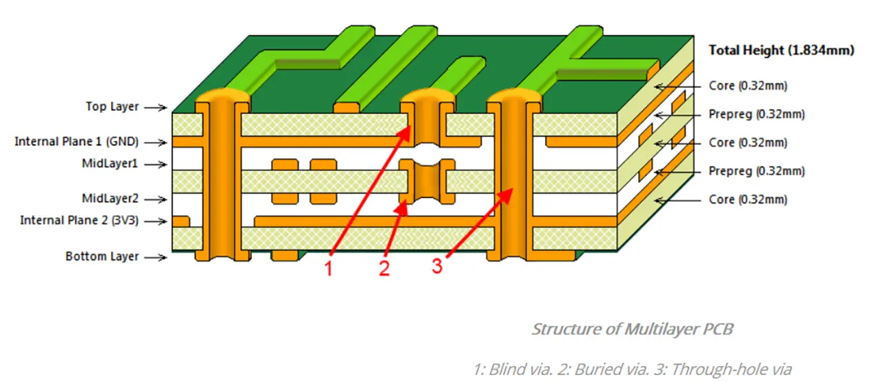
The diagram below shows the stackup structure of a 6-layer 1-step HDI (High-Density Interconnect) multilayer PCB, illustrating its layer stacking and via design:
| Design Challenge | Specific Issues | Solutions |
|---|---|---|
| Signal Integrity | High-speed signal transmission is prone to reflection and crosstalk, leading to signal distortion. The risk of crosstalk increases with more layers. |
|
| Power Integrity | Power planes suffer from noise and voltage fluctuations; multiple voltage supplies are prone to mutual interference, causing chip crashes. |
|
| Wiring & Routability | Increased layers result in limited wiring space; some circuits are difficult to route and may become disorganized. |
|
| Heat Dissipation | High-density layout causes heat accumulation in high-power components, damaging devices and affecting performance. |
|
| Interlayer Alignment & Process | More layers require more lamination cycles (e.g., an 8-layer board needs 7 laminations); copper foil offset between layers (exceeding 30μm may cause short circuits) and cracks during drilling are common. |
|
Key Terminology Notes
- Blind via
- HDI (High-Density Interconnect)
- Differential routing
- Decoupling capacitor
- Thermal via
- Vacuum laminator
The manufacturing process of multilayer PCBs is complex. Parameter deviations or improper operations in any link—from early material selection to final shaping and testing—may affect the quality of finished products. Below are the critical considerations for each core manufacturing stage:
- Choose substrates based on application scenarios: Cost-effective FR-4 substrates are suitable for general consumer electronics, while Rogers materials (low dielectric loss) or polyimide materials (high temperature resistance) are ideal for high-frequency communication devices or aerospace equipment.
- Select copper foil thickness according to current requirements: Thicker copper foil is recommended for high-current power circuits to reduce heat generation.
- Control the resin content of prepregs to avoid impacting interlayer adhesion and signal transmission.
- After transferring circuit patterns to copper-clad laminates via exposure and development, precisely control etching parameters to prevent line width deviations or residual circuits.
- Conduct black oxidation or brown oxidation treatment on the board surface after etching to increase copper foil roughness, enhance interlayer bonding strength, and avoid delamination.
- This is a critical step to stack and bond inner layers, prepregs, and outer copper foils.
- Stack materials in strict accordance with the designed sequence to avoid interlayer misalignment.
- Strictly control lamination parameters: Temperature is typically maintained at 180–220℃, pressure at 3–5MPa, and lamination time must be precisely managed. Imbalanced parameters may cause defects such as bubbles or delamination.
- Prioritize even-layer stacking with a symmetrical structure to minimize board warpage after lamination.
- Use CNC drilling machines to ensure hole position accuracy: The diameter of standard through-holes should be controlled above 0.2mm, with a tolerance of ±0.05mm or less.
- Distinguish application scenarios for through-holes, blind vias, and buried vias to avoid unnecessary complexity.
- Form conductive hole walls through electroless copper plating and electrolytic copper plating; control plating thickness and uniformity.
- Remove residual impurities from hole walls to prevent plating peeling.
- Higher precision is required as outer circuits directly affect component soldering and signal transmission.
- Ensure line width/spacing meets design requirements during photolithography, and avoid defects such as circuit burrs or short circuits.
- HASL (Hot Air Solder Leveling): Cost-effective with good solderability, suitable for consumer electronics.
- Immersion Gold: Flat surface and stable performance, ideal for high-end precision equipment.
- OSP (Organic Solderability Preservative): Low-cost for mild operating environments, but note its poor protection under high temperature and humidity.
- Use CNC routing machines to process the board outline, with cutting precision controlled within ±0.2mm.
- Reserve 3–5mm wide process edges to facilitate subsequent SMT assembly and testing.
- Conduct visual inspection with AOI (Automated Optical Inspection) equipment to detect defects such as open circuits or uneven solder mask.
- Perform electrical performance tests (e.g., flying probe test, ICT test) to ensure impedance deviation is within ±10%.
- Use X-ray inspection for hidden multilayer circuits to verify via quality and interlayer alignment.
- Prepreg
- Black oxidation / Brown oxidation
- Delamination
- Blind via / Buried via
- Electroless copper plating / Electrolytic copper plating
- HASL (Hot Air Solder Leveling)
- Immersion Gold
- OSP (Organic Solderability Preservative)
- AOI (Automated Optical Inspection)
- Flying probe test / ICT (In-Circuit Test)
- Process edge
A multilayer PCB consists of three or more conductive copper layers alternately stacked with insulating prepreg layers, bonded under high temperature and pressure. Unlike single-layer or double-layer PCBs, multilayer PCBs support much more complex wiring, better signal integrity, and greater miniaturization — making them suitable for advanced electronics such as smartphones, servers, and medical devices.
The five most common design challenges are: (1) Signal integrity — preventing reflection and crosstalk in high-speed signals; (2) Power integrity — managing noise and voltage fluctuations across power planes; (3) Wiring and routability — efficiently routing signals across multiple layers; (4) Heat dissipation — preventing heat buildup in high-density layouts; and (5) Interlayer alignment — ensuring accurate layer-to-layer registration during lamination.
Three main via types are used: Through-holes pass through all layers and are the most common; Blind vias connect an outer layer to one or more inner layers without passing through the entire board; and Buried vias connect only inner layers and are not visible from the surface. Blind and buried vias are commonly used in HDI (High-Density Interconnect) designs to save surface space and improve routing density.
The three most widely used surface finishes are: HASL (Hot Air Solder Leveling) — cost-effective and good solderability, ideal for consumer electronics; Immersion Gold (ENIG) — flat surface and stable performance, best for high-end or precision equipment; and OSP (Organic Solderability Preservative) — low-cost and environmentally friendly, but less suitable for high-temperature or high-humidity environments. Your choice should be based on the product's operating environment, soldering requirements, and budget.
Multilayer PCB quality is verified through multiple inspection methods: AOI (Automated Optical Inspection) detects surface defects such as open circuits or uneven solder mask; Flying probe tests and ICT (In-Circuit Tests) verify electrical performance and ensure impedance deviation stays within ±10%; and X-ray inspection is used to examine hidden internal layers, checking via quality and interlayer alignment that cannot be seen from the surface.
FR-4 (epoxy resin fiberglass) is the most cost-effective and widely used substrate, suitable for general consumer electronics. Rogers materials offer low dielectric loss and are preferred for high-frequency communication applications such as 5G or RF devices. Polyimide (PI) substrates provide excellent high-temperature resistance and are used in aerospace and military-grade equipment. The right material depends on the operating frequency, temperature range, and performance requirements of your application.









