
1 / 1
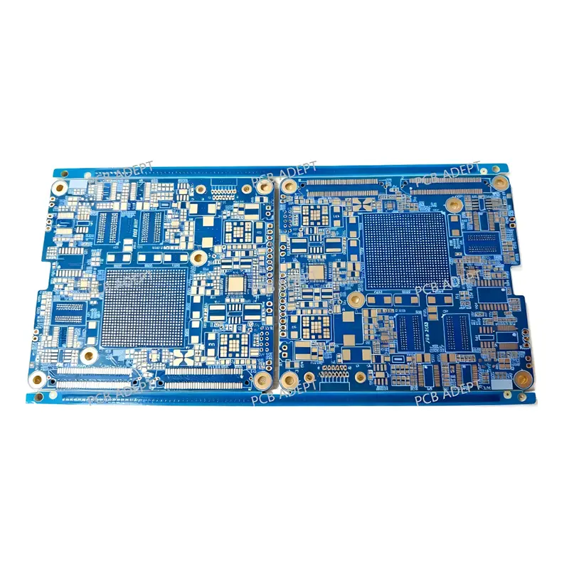
Famous China RF & Microwave PCB Factory - Low Loss, Good Signal, Precise Impedance Control - Suppliers for ≥500MHz Frequency Supplier, Factory
Product Description
What is RF & Microwave PCB?
▶
The core is to control electromagnetic waves, treating PCB wires as transmission lines with characteristic impedance rather than simple electrical connections.
Three Key Design Points
-
1Sheet Material Selection Never use ordinary FR-4. High-frequency dedicated boards with low loss and stable dielectric constant (such as Rogers RO4350B, RT/duroid series) must be selected. This is the cornerstone of performance.
-
➔Impedance and Transmission Lines Precise 50Ω impedance control is essential. Use microstrip lines, striplines or coplanar waveguides and determine the precise line width through calculation/simulation. When laying out, minimize the paths and avoid right angles.
-
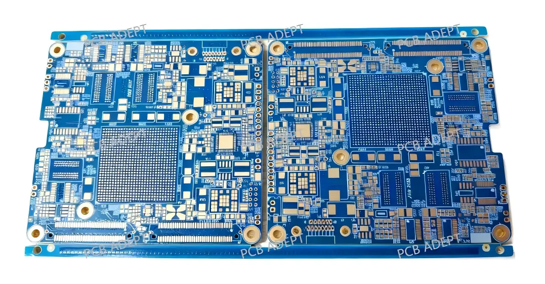
2Grounding and Isolation Provide a complete and solid ground plane to ensure a low-impedance return path. Densely arrange grounding vias (especially on both sides of the transmission line) to suppress resonance and coupling.
-
3Strict Zoning Physically isolate the RF, digital, and power supply areas. When necessary, use shielding covers and via walls.
Key Points of Manufacturing
High-Precision Processing
Strictly control the tolerance of line width and medium thickness to ensure signal integrity across all RF traces.
Surface Treatment
ENIG gold plating is preferred to ensure flatness and high-frequency conductivity for reliable RF performance.
Solder Mask Control
The solder mask layer may affect the impedance, and "window opening" treatment is often adopted for RF traces.
Conclusion
PCBADEPT Technology Company has extensive production experience in RF PCB manufacturing and RF PCB assembly, such as the production of anti-drone equipment, electronic fence equipment, walkie-talkies, etc.
RF PCBs play a very significant role in modern wireless communication devices, and an increasing number of customers are choosing such products.
Send Inquiry
Frequently Asked Questions (FAQ)
Q
What makes RF & Microwave PCB different from standard PCBs?
Unlike standard PCBs, RF & Microwave PCBs treat copper traces as transmission lines with controlled characteristic impedance. They require specialized low-loss materials, precise impedance matching, and strict layout rules to manage electromagnetic wave behavior at high frequencies.
Q
Why can't FR-4 be used for RF & Microwave PCBs?
FR-4 has a relatively high and unstable dielectric constant at high frequencies, along with higher signal loss. For RF and microwave applications, materials such as Rogers RO4350B or RT/duroid series are required because they offer low dielectric loss and a stable dielectric constant across a wide frequency range.
Q
What is the standard impedance used in RF PCB design?
The industry standard characteristic impedance for RF PCB transmission lines is 50Ω. This value is widely adopted because it provides an optimal balance between power handling capability and signal loss. Precise line widths are calculated or simulated to achieve this impedance consistently.
Q
Why is ENIG surface treatment preferred for RF PCBs?
ENIG (Electroless Nickel Immersion Gold) provides an extremely flat and uniform surface, which is critical for RF signal integrity. It also offers excellent high-frequency conductivity and long-term solderability, making it the preferred surface finish for RF and microwave PCB applications.
Q
What applications commonly use RF & Microwave PCBs?
RF & Microwave PCBs are widely used in wireless communication devices, anti-drone equipment, electronic fence systems, walkie-talkies, radar systems, satellite communications, 5G base stations, and other high-frequency electronic applications where signal precision is critical.
Q
How does grounding affect RF PCB performance?
A complete and solid ground plane is essential in RF PCB design. It provides a low-impedance return path for RF signals, suppresses unwanted resonance and electromagnetic coupling between circuit sections, and ensures stable signal transmission. Densely arranged grounding vias, particularly along both sides of transmission lines, are a best practice in RF PCB layout.









