
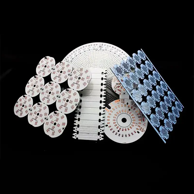
Buy High Thermal Conductivity Aluminum PCB - Top China Suppliers & Factory for Quality Circuit Boards Companies, Factory
Product Description
What is Aluminum PCB?
| Structural layer | Common materials | Core function |
|---|---|---|
| Circuit layer | Electrolytic copper foil ranging from 18 to 140μm | Make circuits and carry the welding of components |
| Insulating layer | Thermal conductive epoxy resin/ceramic filling adhesive | Insulation isolation + heat conduction (thermal conductivity 0.8-8W/m · K) |
| Metal base layer | Aluminum alloy (mainly 6061/5052) | The heat dissipation base quickly disperses the heat conducted by the insulation layer |
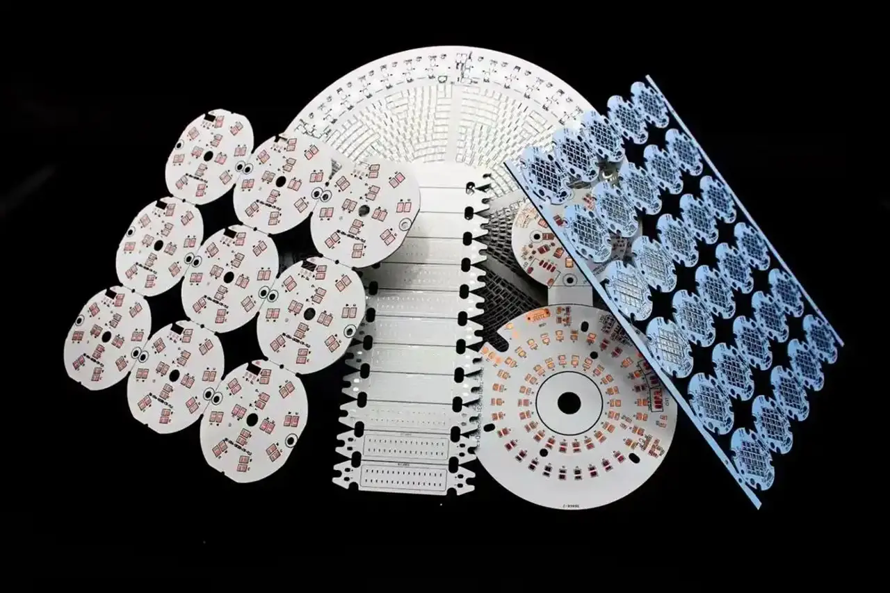
Main Application Scenarios
Core Features
-
🌡️Ultra-High Heat Dissipation The metallic thermal conductivity of aluminum plates quickly transfers heat generated by components (such as LEDs, power transistors) to the external heat dissipation structure, significantly reducing temperature rise and extending service life.
-
⚖️Lightweight + High Mechanical Strength The density of aluminum alloy is much lower than copper and steel. Its bending resistance and impact resistance are superior to ordinary PCBs, making it suitable for portable and vehicle-mounted devices.
-
📐Good Dimensional Stability The coefficient of thermal expansion (CTE) of aluminum alloy can be matched with components, reducing warping and solder joint cracking caused by temperature changes.
-
🛡️Insulation Safety The insulation layer can withstand high voltage (common withstand voltage ≥3000V AC), preventing short circuits between the circuit and the aluminum plate.
Key Design and Manufacturing Points

Design Considerations
Heat dissipation pads: Under the pads of high-power devices, "heat-conducting pads" should be designed and connected to the aluminum plate through metallized vias (≥0.3mm).
Line width & current: The line width should be designed according to "1A current corresponding to 0.3mm line width (copper thickness 35μm)" to avoid heat generation.
Edge treatment: Burrs on aluminum plate edges can puncture the insulation layer — chamfering (≥0.5mm) treatment is required.

Manufacturing Process
Insulation layer bonding: High-temperature and high-pressure (180℃/3MPa) bonding is required to ensure the insulation layer is free of bubbles and peel strength is ≥1.0N/mm.
Surface treatment: Tin plating/nickel-gold plating is preferred; OSP (organic film has poor heat resistance) should be avoided.
Forming method: CNC milling is adopted (instead of die-cutting for ordinary PCBs) to ensure the flatness of aluminum plate edges.









