
Buy China Flexible PCB Suppliers - Thin, Lightweight, and Bendable for Consumer Electronics - Factory Direct Quality Company, Pricelist
Product Description
The Main Functions Are Reflected In
▶ Realize Three-Dimensional Wiring
Can be bent and folded inside the device, greatly enhancing space utilization and design freedom.
▶ Promoting Miniaturization
Thin and light characteristics are the key for smartphones and wearable devices to achieve lightness and portability.
▶ Enhance System Reliability
Reduce connectors and solder joints to be more durable in vibrating and bending environments.
Far-Reaching Impact
It has directly given rise to innovative product forms such as foldable screen mobile phones and wearable devices, and has become an indispensable cornerstone for the high-end development of fields such as automotive electronics, medical equipment, and aerospace. Flexible PCBs have profoundly transformed the design concepts and industrial landscape of electronic products by endowing them with "flexibility" and "deformability" capabilities.
What is Flexible PCB (FPC)?
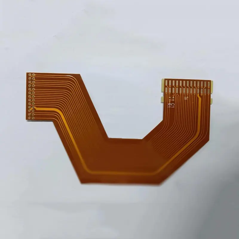
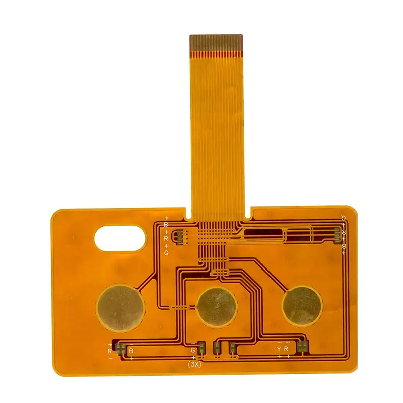
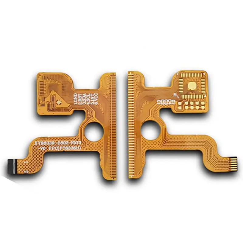
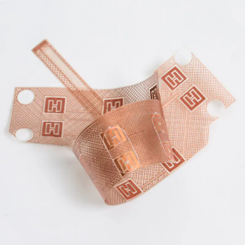
Flexible PCB, whose full name is flexible printed circuit board, is commonly known as "soft board". You can imagine it as a kind of "flexible electronic circuit" or "circuit cloth". It is a "relative" of the common green, hard computer motherboard (rigid PCB) we often see, but the core material is completely different.
- ▶ The material is soft: Its substrate is not hard glass fiber but a flexible plastic film such as polyimide, which is heat-resistant and can be repeatedly bent.
- ▶ Bendable and foldable: It can be bent, wound and folded in three dimensions to adapt to various narrow or irregular spaces.
- ▶ Thin and light: Much thinner and lighter than rigid PCBs.
- ▶ Smartphones / Foldable phones: The "flat cables" connecting screen, camera, buttons and battery are mostly flexible PCBs. Foldable phone hinges require FPC capable of withstanding hundreds of thousands of bends.
- ▶ Wearable devices: Smartwatches, bracelets and health patches need to fit the curves of the human body.
- ▶ Notebook computers: The "link" connecting the motherboard and the screen.
- ▶ Automotive electronics: LED headlights, central control screens, various sensors and complex wiring harnesses in compact spaces.
- ▶ Precision medical equipment: Endoscope capsules and pacemakers with extremely high requirements for space and reliability.
- ▶ Aerospace: The "sinews and bones" for satellites and aircraft, reducing weight and adapting to complex cabin layouts.
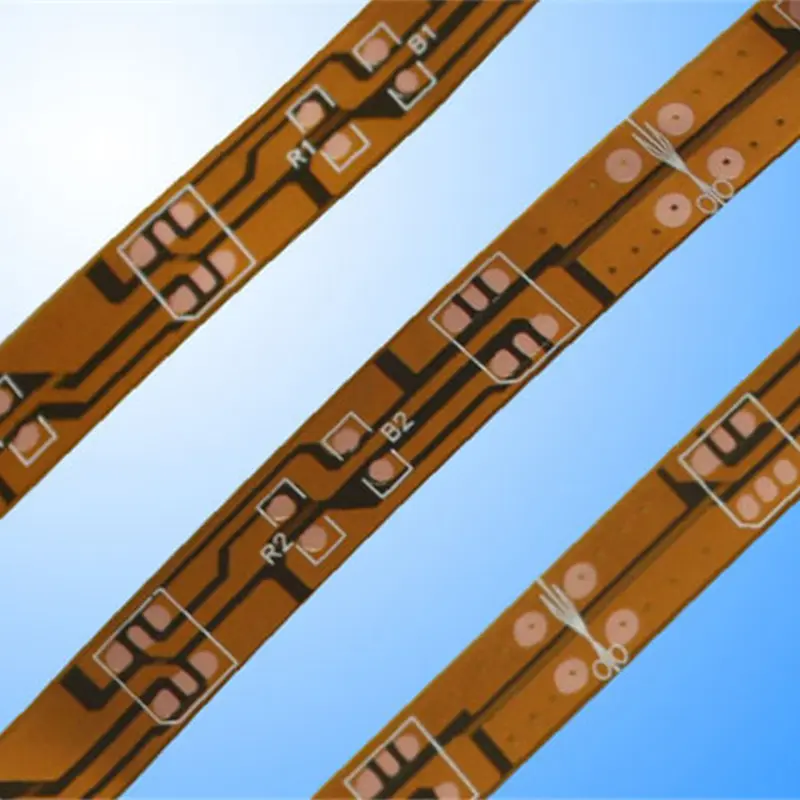
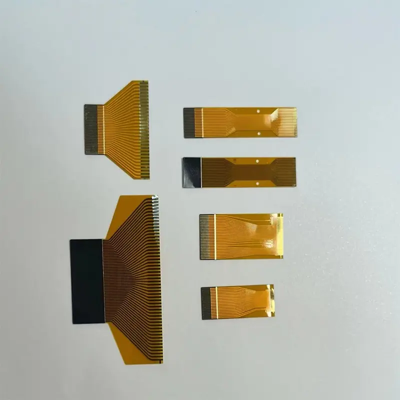
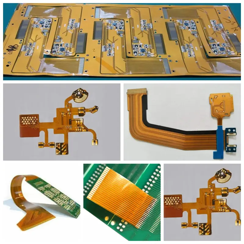
Normal Types of Flexible PCB
How to Design Flexible PCB?
Flexible PCB is widely used in consumer electronics, automotive electronics, medical equipment and other fields due to its bendable, thin and light, and bending-resistant characteristics. Its design needs to take into account the characteristics of flexible substrates, mechanical reliability and electrical performance.
- Substrate selection: Commonly used PI (polyimide) base material (temperature resistance -200°C to 260°C, excellent bending resistance), supplemented by PET for low-requirement scenarios. PI covering film is preferred to match the bending characteristics.
- Thickness matching: Flexible substrate thickness (25μm, 50μm PI) should match bending radius and load-bearing requirements. Electrolytic copper (good ductility) is preferred; recommended thickness 12μm or 18μm. Avoid thick copper (≥35μm) as it increases bending stress.
- Structural design: Single layers for simple wiring; multi-layers need bonding layer (acrylic adhesive). For high-frequency/high-bending scenarios, glue-free (Rigid-Flex) boards are preferred. Rigid-to-flex zone junctions should be chamfered (≥0.3mm) to prevent stress cracking.
- Line width / spacing: Flexible zone line width ≥0.1mm, spacing ≥0.1mm. For high-current traces, widen width (e.g., 1A current → ≥0.3mm width, 18μm copper) to prevent heating.
- Routing form: Prohibit right-angle / acute-angle routing — use arc transitions (fillet radius ≥0.1mm). Wiring in bending areas should be parallel to the bending direction.
- Layout optimization: No components in the flexible area. Place components in the rigid area, at least 1mm from the flexible zone edge. Symmetrical layout reduces inter-layer stress differences.
- Minimum bending radius: Must meet "bending radius ≥5× total board thickness". For dynamic bending scenes, increase to 10× total thickness.
- Bending life: Common flexible board dynamic bending life ≈100,000 times. Use bend-resistant base materials for high-reliability scenarios.
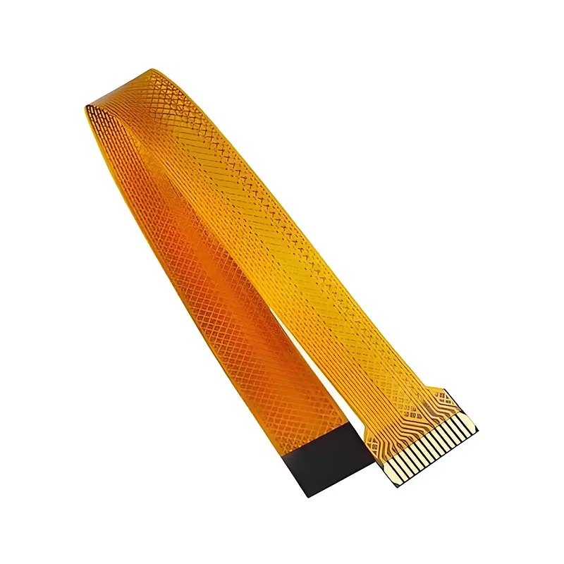
- Stress relief: Use grid-shaped copper in bending areas (not solid copper). Add polyimide reinforcing ribs (25–50μm thickness) in high-stress areas.
- Pad specification: No pads in the flexible zone. If welding is required in the flexible zone, add a rigid reinforcing plate (FR-4 or stainless steel) covering ≥0.5mm outside the pad. Use rectangular pads with rounded corners (radius ≥0.1mm).
- Through holes: Prohibited in the flexible zone; must be in the rigid zone. Metallized via hole diameter ≥0.2mm, copper plating thickness ≥8μm.
- Positioning holes: Keep away from bending area. Hole diameter tolerance ±0.05mm; chamfer edges to prevent scratching.
- Covering film design: Must completely cover flexible area traces. Window edge to trace distance ≥0.1mm. Recommended covering film thickness in bending area: 25μm.
- Bending process: Cold bending (room temperature) required. Hot bending strictly prohibited. Bending angle must not exceed 180°.
- Surface treatment: OSP or nickel-gold plating preferred for the flexible zone. Avoid tin spraying (high temperature reduces substrate flexibility).
- Impedance control: For high-frequency boards (5G, RF), calculate impedance (50Ω, 100Ω differential). Impedance deviation in bending area must be within ±10%.
- Grounding design: Design a complete grounding layer to reduce electromagnetic interference. Keep grounding layer continuous; avoid disconnection in the bending area.
Flexible PCB Manufacturing Processes and Controls
The manufacturing process of flexible PCBs is one of the most delicate and complex fields in electronic manufacturing. The core difficulty lies in dealing with extremely thin, soft, deformable and environmentally susceptible materials.
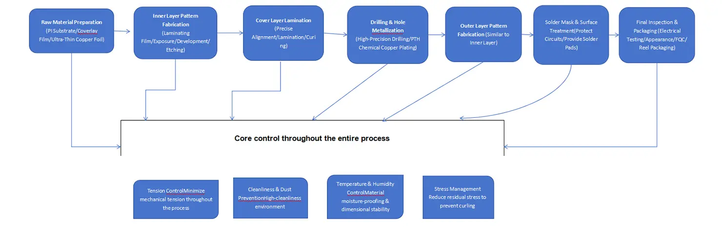
I. Detailed Explanation of Core Manufacturing Process Flow
- Cutting and cleaning: Cut the roll-shaped PI substrate and copper foil in a constant temperature and humidity environment. Clean immediately to remove oil stains and particles.
- Dry film application / photoresist coating: Apply a single layer of photosensitive resist (dry film) onto the copper foil.
- Exposure and development: Expose the film with a line pattern to UV light, then develop to protect the required line pattern and wash away unexposed resist.
- Etching: Use chemical solutions (e.g., acidic copper chloride) to etch away unprotected copper, forming fine copper circuits. Etching factor control requirements are extremely high for fine-line accuracy.
- Film removal and cleaning: Remove the resist layer to obtain the exposed inner circuit pattern.
- Surface treatment: Micro-etching or chemical treatment on the copper circuit to enhance adhesion with the covering layer.
- Coating alignment and lamination: Align the PI covering film (with openings to expose solder pads) via precise optical alignment, then perform hot-pressing curing. No bubbles, no wrinkles, and precise alignment are essential.
- Drilling: Use high-speed, low-feed drilling rigs with specially designed covers and pads to prevent burrs, nail heads or material tearing.
- Pre-treatment and electroless copper plating: Activate hole walls with plasma or potassium permanganate solution, then deposit a thin layer of chemical copper to provide a conductive substrate for subsequent electroplating.
- Outer layer pattern transfer: Film application, exposure, development, pattern electroplating, copper thickening, and etching form the outer layer circuits and through-hole connections.
- Solder mask and surface treatment: Apply flexible solder mask ink; pads undergo surface treatment (chemical nickel-gold, OSP or electroplated hard gold for gold fingers).
- Shape processing: Final shape cut via precision die punching or CNC milling. Strict mold clearance and milling cutter control to prevent delamination and burrs.
- Electrical testing and final inspection: 100% open and short circuit electrical tests (flying probe tests), visual inspection, dimensional measurement and reliability spot checks (bending test, solderability test).
II. Four Core Control Dimensions Running Through the Entire Process
Tension Control
All conveying rollers must achieve minimum or zero tension. Excessive stretching causes permanent deformation, inaccurate alignment, dimensional deviations and microcracks.
Cleaning & Dust-Proof Control
Key processes (exposure, lamination, covering) must be in an environment with cleanliness level of 1,000 or higher. Tiny dust causes circuit notches, short circuits or open circuits.
Temperature & Humidity Control
Maintain constant temperature and humidity (22±2°C, 50±5%RH). All hygroscopic materials must be strictly baked before use to prevent plate cracking and delamination.
Stress Management
Design symmetrical stacked structures. Adopt slow cooling after lamination. Carry out stress release baking when necessary to prevent the finished board from warping and curling.
The Application of Flexible PCBs in 2026
Looking ahead to 2026, the application of flexible PCBs (FPCs) and rigid-flex boards will become more extensive and in-depth. The core driving forces come from innovation of equipment forms, demand for performance improvement, and the explosion of emerging markets.
1. Consumer Electronics: The Core of Form Revolution
Folding/curling/stretching screen devices: FPCs will serve as the "neural network" for hinges and screens. Foldable phone forms will be more diverse (three-fold, rollable), with higher requirements for bending reliability, thinness and signal integrity.
AR/VR devices: Flexible PCBs are key to achieving high-density wiring and sensor integration in thin and light helmets and smart glasses.
New wearables & "electronic skin": Smart bracelets/watches will integrate more health sensors (e.g., continuous blood glucose monitoring). Flexible patches for health monitoring will enter the consumer market.
2. Automotive Electronics: "Blood Vessels" of Intelligence
Intelligent cockpits and displays: Large-sized, irregular-shaped, height-adjustable automotive displays will extensively employ rigid-flex panels and FPCs.
ADAS and autonomous driving: Increasing cameras, millimeter-wave radars and lidar sensors require lightweight FPCs for high-speed signal transmission along complex vehicle body curves.
Battery management systems: FPC replacement of traditional wiring harnesses in EV battery packs is a clear trend, enabling more accurate voltage/temperature monitoring and higher integration.
3. Medical & Healthcare: From Diagnosis to Treatment
Implantable and ingestible devices: Micro-implantable devices for cardiac monitoring and nerve stimulation require highly integrated flexible/rigid-flex combined circuits for ultimate miniaturization and biocompatibility.
High-end wearable medical devices: Hospital-grade continuous vital sign monitoring patches will become more widespread, with flexible PCBs ensuring comfort, accuracy and wireless connectivity.
4. Communication & Computing: Performance Upgrade
5G-Advanced / 6G and millimeter-wave devices: High-frequency communication requires extremely low signal loss. Flexible circuits using LCP substrates will be the preferred solution for millimeter-wave antenna modules and high-speed connectors.
Advanced packaging and chip interconnection: FPC technology will be more widely applied to chip-level interconnection, such as the interposer layer in 2.5D/3D packaging or the rewiring layer in fan-out packaging.
5. Robots & Human-Machine Interaction
Bionic and collaborative robots: Flexible sensors and circuits integrated into robot "fingers" and "skin" will endow them with more sensitive touch and adaptive grasping capabilities.
Structural electronics integration: FPC will integrate with structural components to form "structural electronics" — the product casing itself becomes part of the circuit, achieving ultimate space savings and functional integration.
Core Trends Summary for 2026
Technology integration: FPC is integrating with sensors, antennas, heat dissipation films and light-emitting components, becoming a "multi-functional system module".
Material innovation: LCP and modified PI substrates will be popularized for higher frequencies, greater heat resistance, and better bending performance.
Market penetration: With cost optimization and process maturation, FPC will rapidly penetrate from high-end to mid-range consumer electronics and mainstream vehicle models.
Conclusion
Flexible PCB (FPC) is a silent revolution in electronic interconnection technology. It is not only a material that makes electronic devices "softer" and "thinner", but also a fundamental enabling technology that drives product innovation, enhances system performance, and gives rise to brand-new application scenarios. Its future development will continue to follow the direction of "thinner and lighter, more reliable, higher frequency and speed, and higher integration", deeply embedded in every key electronic node of the intelligent society, and its importance will increase day by day.









