
High-Frequency, Multilayer & Precision Prototyping Solutions
Explore our primary prototyping product lines, featuring rapid 24-to-48 hour turnaround, advanced impedance control, and IPC Class 2/3 certified manufacturing lines.

Buy High Density Interconnect PCB Suppliers in China - Quality HDI PCB from Reliable Factory Pricelist, Factories
Explore HDI Specifications
OEM High-Quality 1-60 Layers Multilayer PCB from China Suppliers - Fast Lead Time 48 Hours, IPC2 Grade Factory Manufacturer, Suppliers
Explore Multilayer Builds
China China Flexible PCB Suppliers - Thin, Lightweight, and Bendable Solutions from a Leading Factory Company, Quotes
View Flexible PCB Solutions
China China PCB Prototype Suppliers: Fast Manufacturing Solutions from Leading PCB Factory for Modern Electronics Manufacturers, Manufacturer
Request Rapid Prototyping
China China Suppliers for RF & Microwave PCBs - Low Loss, Good Signal, and Impedance Control for ≥500MHz Frequency Factory Factories, Factory
Inquire RF/Microwave Specs

Buy China Suppliers and Factory for Raspberry Pi HAT: Enhance Your Projects with Versatile Expansion Boards Supplier, Companies
View Expansion Assemblies
ODM Rapid PCB Prototyping and Validation by China Suppliers: Quality Factory Solutions for Modern Electronics Company, Quotes
Discover ODM ValidationEmpowering Global R&D with Full-Cycle Traceability
Shenzhen ICSLOVE Technology Co., Ltd. (operating internationally as PCB ADEPT) operates an advanced 8,000 m² smart manufacturing plant in Shenzhen’s core industrial cluster. We bridge the engineering gap between rapid NPI iterations and mass-production reliability.
Turnkey Manufacturing Footprint
Founded in 2020 in Bao'an District, Shenzhen, PCB ADEPT integrates bare board fabrication, high-precision surface mount technology (SMT), dual-in-line packaging (DIP), and complete box-build electro-mechanical box assemblies. Our continuous investment in 6 automated SMT lines and 4 DIP wave soldering lines provides robust scaling flexibility.
- End-to-end Manufacturing Execution System (MES) barcoding for 100% component-level traceability.
- Seamless transition from 1-500 piece prototyping batches to continuous high-volume contracts.
Rigorous Defect Prevention & DFM
Rather than merely catching errors post-production, our Design for Manufacturability (DFM) and Design for Assembly (DFA) audits commence the moment Gerber data, stack-ups, and BOMs are ingested. We run simulated solder reflow thermal profiling, verify annular ring aspect ratios, and mitigate acute copper etching slivers.
- In-line Solder Paste Inspection (SPI) coupled with Pre/Post-reflow 3D AOI & Real-time X-Ray (AXI).
- Complete Flying Probe, In-Circuit Testing (ICT), and customized Functional Circuit Testing (FCT).
Next-Gen Interconnect Architectures: From Subtractive to mSAP & SLP
As electronic architectures demand greater clock frequencies, denser ball-grid arrays (BGAs), and minimal dielectric insertion loss, conventional PCB manufacturing must evolve. Our engineering roadmap addresses the physical boundaries of signal integrity, thermal dissipation, and ultra-miniaturized geometries.
mSAP & Substrate-Like PCB (SLP)
Subtractive chemical etching inevitably introduces trapezoidal trace profiles with severe undercut issues at line widths/spacing below 50/50 μm. PCB ADEPT has engineered a reliable Modified Semi-Additive Process (mSAP) roadmap, delivering rectangular trace cross-sections down to 25/25 μm, enabling fine-pitch IC packaging and ultra-compact wearable devices.
- Laser direct imaging (LDI) with ±8 μm registration accuracy.
- Micro-via aspect ratios exceeding 1:1 via advanced copper electroplating.
Ultra-High-Speed Signal Integrity
With the proliferation of PCIe 6.0/7.0 interfaces and 112G/224G PAM4 transmission, substrate material selection dictates eye-diagram opening and jitter margins. We utilize specialized ultra-low loss hydrocarbon, PTFE, and polyphenylene ether (PPE) laminates (e.g., Rogers RO4350B, Megtron 6/7/8, Taconic), standardizing back-drilling to eliminate resonant stub reflections.
- Tight impedance tolerance controlled within ±5% across high-layer backplanes.
- Surface roughness mitigation using Very Low Profile (VLP) and HVLP copper foils.
Embedded Die & Heterogeneous Hybrids
To accommodate intense localized thermal loads, our production facility pairs heavy copper busbar technology (up to 10 oz) with hybrid rigid-flex configurations. We are deploying embedded passive and active die cavities directly inside inner lamination layers, shortening loop inductances for next-generation gallium nitride (GaN) and silicon carbide (SiC) switching topologies.
- Copper coin bonding and thermal via arrays for conduction paths exceeding 380 W/m·K.
- Sequential electrochemical surface finishes: ENIG, ENEPIG, and selective immersion gold.
Mission-Critical Electronics: Configured for Stringent Environments
Different industry verticals cannot be served with generic fabrication tolerances. PCB ADEPT structures tailored manufacturing cells and testing matrix protocols to meet sector-specific environmental, mechanical, and regulatory demands.
Automotive ADAS & EV Power Electronics
Automotive electrification demands unprecedented heat resistance and zero-defect tolerance. Our quick-turn prototyping services support 77GHz radar sensor boards, battery management systems (BMS), and onboard charging systems (OBC). Built strictly in accordance with IPC Class 3 and automotive reliability standards, boards endure rigorous thermal shock cycling (-40°C to +150°C) without delamination.
Aerospace & Anti-Drone Systems
In tactical electronic countermeasure (ECM), UAV command-and-control links, and satellite transceiver modules, signal purity and thermal dissipation under sustained high-wattage RF transmission are vital. We manufacture multi-layer hybrid RF boards incorporating Rogers PTFE substrates pressed symmetrically with FR-4 core layers, finished with electrolytic nickel/gold to eliminate passive intermodulation (PIM).
Medical Diagnostic Devices & Class III Monitoring
From implantable patient sensors to clinical diagnostic ultrasound hardware, medical applications require absolute trace cleanliness, lead-free RoHS biocompatibility, and extreme ionic purity. Our assembly lines feature automated ultrasonic aqueous deionized wash cycles ensuring ionic contamination remains far below 0.75 μg/cm² NaCl equivalent.
Industrial Automation 4.0 & Edge Compute
Factory-floor PLC controllers, edge computing gateways, and robotics sensor arrays operate in hostile environments replete with vibration, moisture, and EMI noise. We offer conformal coating (acrylic, polyurethane, silicone) coupled with selective potting. Our engineering staff supports reverse-engineering and component-drop replacement for obsolete legacy industrial boards.
Telecom Infrastructure & 5G mmWave
Supporting multi-beam phase array antennas, 5G small cells, and massive MIMO base stations. We construct backplanes up to 60 layers featuring blind and buried micro-vias, staggered via-in-pad structures (VIPPO), and exact resonant impedance tracking for frequencies reaching past 77 GHz.
Consumer Smart Devices & IoT Hardware
Rapid design turnaround, extreme cost-down optimization, and ultra-miniature form factors are essential for commercial consumer IoT electronics. Leveraging high-speed Yamaha SMT placement mounters, we mount 01005 passive resistors and ultra-fine pitch BGAs (0.35 mm pitch), providing seamless integration for wearables and Raspberry Pi expansion modules.
China Factory 4.0: Supply Chain Agility & Prototyping Velocity
Shenzhen is the undisputed epicentre of the global hardware revolution. Situated within Bao'an District, PCB ADEPT harnesses the world’s most concentrated component procurement corridor, eliminating long-lead bottlenecks and accelerating physical prototype fabrication.
One-Hour Component Sourcing Radius
Surrounded by premier global silicon distribution networks and official franchises for Texas Instruments, Analog Devices, STMicroelectronics, Microchip, Murata, and TE Connectivity, our dedicated procurement specialists resolve shortage crises within hours. We maintain extensive on-site buffer inventories of certified passive components, enabling instant kitting for fast-turn projects.
Manufacturing Execution System (MES)
Every incoming component reel, raw copper substrate, and chemical bath is digitized into our factory-wide MES database. By tracking paste batch numbers, stencil tension values, reflow peak zone thermal curves, and post-AOI coordinate data, our clients receive full digital twin production reports confirming complete process repeatability.
Agile Quick-Response Cells (QRC)
To safeguard urgent prototyping timelines from getting stalled behind 100,000-piece commercial runs, PCB ADEPT reserves dedicated Quick-Response Cells. These high-speed SMT and bare-board lamination lines specialize strictly in rapid NPI turnarounds (1 to 500 boards), ensuring your firmware and mechanical engineers hit validation schedules on time.
State-of-the-Art SMT, DIP & Testing Stations
Explore our Shenzhen manufacturing floor, where automated robotics, multi-zone nitrogen reflow ovens, and intelligent optical inspection platforms guarantee zero-defect PCBA execution.

Incoming Quality Control (IQC)
Incoming silicon, ICs, passives, and raw copper laminates are verified with optical microscopes, digital calipers, and solderability testers to ensure zero counterfeit or damaged components enter production.
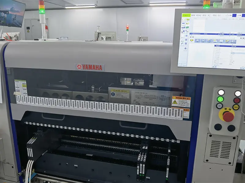
YAMAHA SMT Placement Fleet
Equipped with 6 high-speed YAMAHA surface mounters handling micro-passives from 01005 to fine-pitch BGAs (0.35 mm pitch), QFNs, and odd-form connectors with precision placement repeatable to ±0.025 mm.
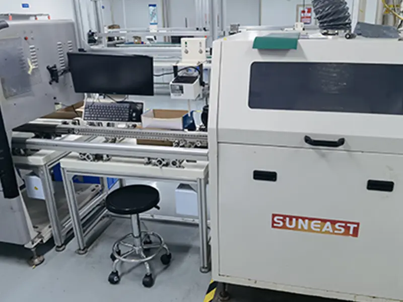
Pre-Reflow Automated Optical Inspection
Pre-reflow AOI catches tombstoning, trace misalignment, skew, missing parts, and inverted polarities before soldering occurs, avoiding costly rework and maximizing solder integrity.
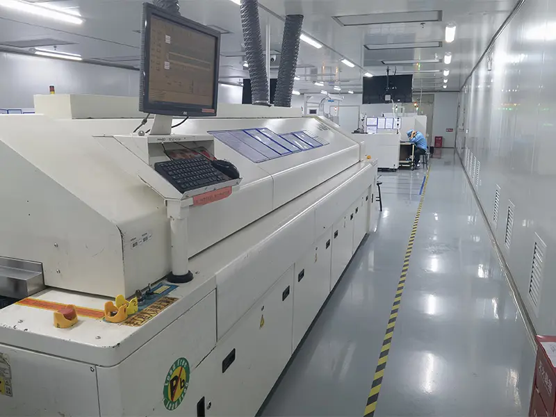
Multi-Zone Nitrogen Reflow Ovens
Multi-zone forced-convection lead-free reflow ovens customized for specific thermal profiles. Guarantees ideal wetting without blistering delicate flex circuits or warping thick high-layer boards.
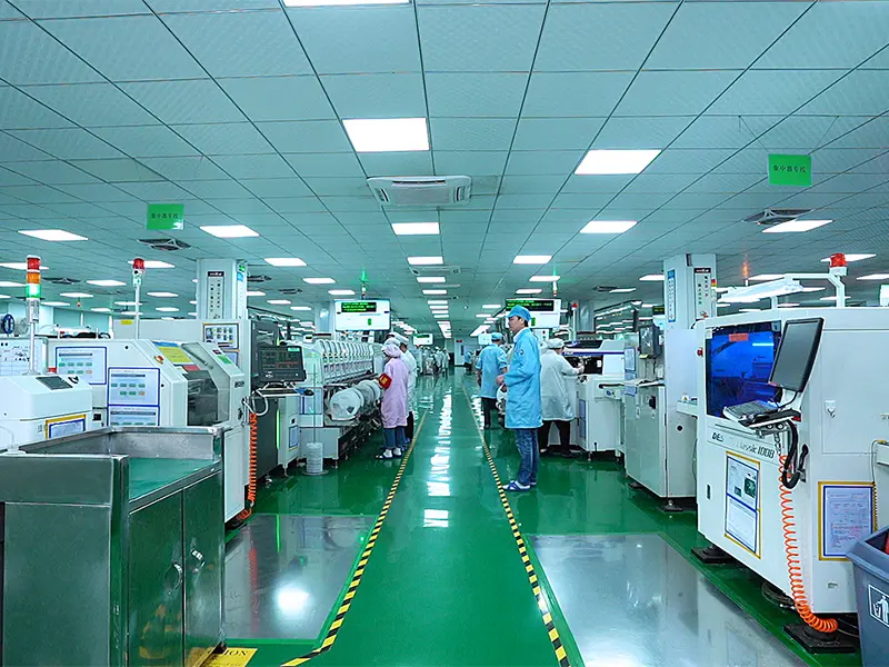
Climate-Controlled SMT Environment
Class 100,000 cleanroom-level workshop maintains positive pressure, constant 40-60% relative humidity, and active electrostatic discharge (ESD) ground loops for static-sensitive semiconductor arrays.
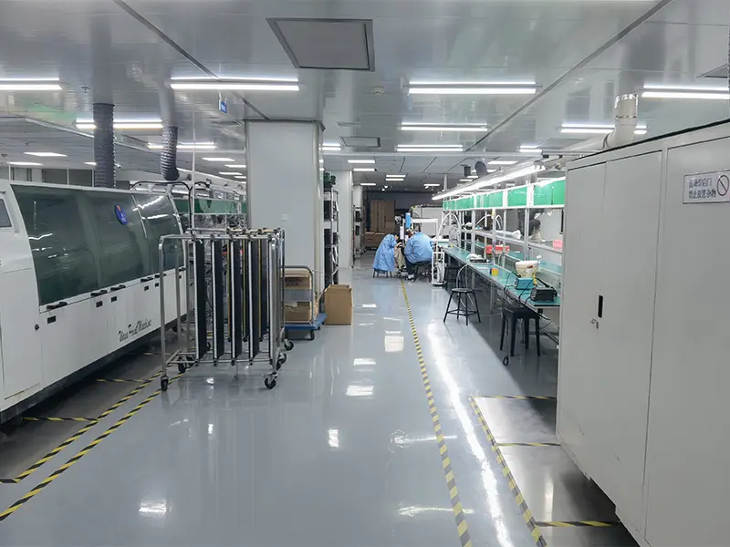
DIP Through-Hole & Selective Wave Solder
4 dedicated dual-in-line packaging (DIP) lines with selective wave soldering nozzles and specialized pallets protect surface mount components while soldering heavy-duty connectors and relays.
Localization Support & Global Quality Standards
International electronics procurement hinges on transparent compliance, stringent international certifications, and seamless communication. PCB ADEPT aligns fabrication processes with North American and European regulatory frameworks.
IPC Class 2 & Class 3 Fabrication
Every circuit board and solder fillet is evaluated against IPC-A-600 (bare board acceptability) and IPC-A-610 (electronic assembly acceptability). For medical, defense, and aerospace clients, we support Class 3 high-reliability builds requiring uninterrupted electrical uptime and zero pore or void compromise.
RoHS, REACH & UL 94V-0 Certified
We provide complete material substance declarations confirming total compliance with EU Directive 2015/863 (RoHS 3) and SVHC chemical lists under REACH. All laminates, soldermasks, and legends conform to UL 94V-0 flame retardancy ratings, stamped with authentic UL markings for immediate customs import clearance.
Bilingual DFM Engineers & DDP Logistics
Hardware procurement headaches often stem from linguistic and timezone friction. PCB ADEPT pairs every client with a dedicated English-fluent DFM project engineer. We offer complete Delivered Duty Paid (DDP) door-to-door air freight via DHL, FedEx, and UPS, managing customs tariffs, export declarations, and tax filings.
| Manufacturing Parameter | Standard Capability | Advanced / Quick-Turn Quick-Response Limit |
|---|---|---|
| Layer Count | 1 – 32 Layers | Up to 60 Layers (Backplanes, Complex Multilayers) |
| Min. Trace Width / Spacing | 3.0 mil / 3.0 mil (75 μm / 75 μm) | 1.8 mil / 1.8 mil (45 μm / 45 μm via mSAP) |
| Min. Mechanical Drill Hole | 0.20 mm (8 mil) | 0.15 mm (6 mil) |
| Laser Micro-Via Diameter | 0.10 mm (4 mil) | 0.075 mm (3 mil) via UV/CO2 Laser |
| Base Laminate Materials | Standard FR-4, High-Tg FR-4 (IT180A, S1000-2) | Rogers, Taconic, Megtron 6/7/8, Polyimide, Aluminum / Copper base |
| Surface Finishes | HASL, Lead-Free HASL, ENIG (Immersion Gold) | ENEPIG, Hard Gold Plating (30 μ"), Immersion Silver, OSP |
| Component Pitch & Sizes | 0201 Passives, 0.40 mm Pitch BGA | 01005 passives, 0.35 mm pitch fine BGA, QFN, WLCSP |
| Inspection & Validation | AOI, Flying Probe, Electrical Testing, Visual QA | 3D SPI, 3D AOI, Real-time X-Ray (AXI), FCT, Ionic Contamination Testing |
Total Cost of Ownership (TCO) & Strategic BOM Optimization
Strategic procurement executives understand that the cheapest upfront board quotation often results in catastrophic project costs if components are counterfeit, solder joints void, or production deliveries slip. Here is how PCB ADEPT safeguards your margins.
Active BOM Cost-Down Proposals
During initial DFM review, our component engineering team audits your Bill of Materials against current lifecycle availability. We identify single-source choke points, end-of-life (EOL) semiconductors, and suggest drop-in pin-compatible alternatives from tier-1 domestic and Asian manufacturers, frequently unlocking 10% to 25% direct component savings.
Turnkey Box Build & System Integration
Juggling separate vendors for bare boards, SMT assembly, injection molded enclosures, CNC aluminum casings, wire harnesses, and final firmware flashing generates administrative chaos and accountability finger-pointing. PCB ADEPT acts as your single accountable EMS partner, delivering fully assembled, aged, and retail-packaged finished products.
Pilot-Run Validation to Mass Scale
Our manufacturing ecosystem eliminates setup barriers: pilot-runs of 5 to 500 boards utilize the exact high-end SMT lines and thermal profiling configurations that will later govern your 100,000-unit continuous runs. This eliminates re-qualification risks when scaling up from R&D proof-of-concept to volume market launch.
Trusted by Electronics Brands Worldwide
Over 500 technology enterprises across North America, Europe, East Asia, and the Middle East rely on PCB ADEPT for rapid product engineering and mission-critical electronics production.










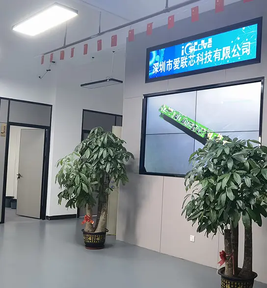
Relocated to Anda Electronic Industrial Zone
Since May 2025, Shenzhen ICSLOVE Technology Co., Ltd. has fully centralized its operational headquarters on the 5th Floor, Area B, Building 3, Anda Electronic Industrial Zone, Fuhai Subdistrict, Bao'an District. Our facility features advanced cleanroom zones, expanded warehouse capacities, and high-speed fiber data links connected to global CAD repositories.

Comprehensive Quality Verification Protocols
We believe that quality cannot be tested into a finished board; it must be built into each process step. From solder paste viscosity tests and laser stencil measurement to post-solder peel-strength assessments, our quality assurance protocols ensure your prototypes function consistently right out of the box.
Frequently Asked Questions: Procuring PCB Prototyping
In-depth answers to technical inquiries concerning manufacturing limits, file preparations, intellectual property safeguards, and fast-turn timelines.
What is the minimum order quantity (MOQ) and turnaround time for rapid prototypes?
What engineering files are mandatory for quoting and launching production?
How does PCB ADEPT prevent counterfeit or defective electronic components?
Can you handle complex HDI stack-ups and advanced high-frequency laminates?
How are intellectual property (IP) and proprietary firmware protected?
What testing options are conducted prior to product delivery?
Explore Specialized Production & Expansion Boards
Choose from our specialized heavy copper, high-frequency, flexible, and custom expansion board configurations manufactured for immediate global delivery.

Famous High Frequency PCB Solutions from China Suppliers and Factory: Minimize Signal Loss and EMI Issues Pricelist, Factory
Review High-Frequency Specs
Buy High-Quality Heavy Copper PCBs from China Factory: Ideal for Power Converters and Strong Current Applications – Top Suppliers Company, Factory
View Heavy Copper Boards
ODM High-Quality Multilayer PCB from China Suppliers & Factory | 1-60 Layers, IPC2 Grade, Fast 48-Hour Lead Time Manufacturers, Quotes
Explore Multilayer Quotes
OEM China Flexible PCB Suppliers - Bending, Folding, Lightweight Connections for Consumer Electronics Factory Manufacturers, Manufacturer
View Flex PCB Options
China High-Quality RF & Microwave PCBs from China Suppliers - Precision Impedance Control for ≥500MHz Frequency Supplier, Companies
Inquire Microwave Specs
Famous China Suppliers of Raspberry Pi HAT: Enhance Your Development with Our Factory's Quality Expansion Boards Companies, Company
Request Expansion Boards
China China Raspberry Pi HAT - High-Quality Expansion Boards from Trusted Suppliers and Factory Quotes, Factories
Explore Raspberry Pi HATs
China High-Density Interconnect PCBs from China | Trusted Suppliers and Factory for Quality HDI Circuit Boards Company, Factory
Get Instant HDI QuotationAccelerate Your Next Hardware Release
Send your Gerber files, Bill of Materials, and stack-up requirements today. Receive comprehensive DFM/DFA engineering feedback and an itemized turnkey quotation within 2 to 24 hours.