

Tier-1 SMT Production Line
Featured Automated PCB Fabrication & PCBA Solutions
Explore precision-engineered bare boards and turnkey SMT assemblies manufactured with high-speed automated lines under IPC-A-610 Class 2/3 quality control standards.

Buy Raspberry Pi HAT: Affordable Mini Computer for IoT and Smart Home Projects - China Factory Suppliers Manufacturers, Factory
Configure Specs & RFQ
ODM Heavy Copper PCB for Power Converters - High Current Capacity, Excellent Heat Dissipation | China Suppliers & Factory Manufacturers, Factories
Configure Specs & RFQ
Famous Flexible PCB from China Suppliers - Lightweight, Bendable and Foldable Solutions from Our Factory Manufacturers, Factories
Configure Specs & RFQ
Buy RF & Microwave PCB Manufacturer, Suppliers
Configure Specs & RFQ
China Heavy Copper PCB for Power Converters - China Suppliers' Superior Factory Products for Enhanced Heat Dissipation and Current Capacity Supplier, Pricelist
Configure Specs & RFQ
ODM High TG PCB Suppliers and Factory in China for Automotive, Aerospace, and Defense Industries (TG150, TG170, TG180, TG260, TG300) Manufacturer, Pricelist
Configure Specs & RFQ
China High Frequency PCB Solutions from Trusted China Suppliers | Quality Manufacturing Factory Company, Pricelist
Configure Specs & RFQ
Global Commercial Status
The Global Landscape of Automated PCB Assembly Manufacturing
How automation, algorithmic vision inspection, and digitalized supply chains are redefining electronic contract manufacturing across North America, Europe, and Asia-Pacific.
99.8%
First-Pass Yield
01005
Micro-SMT Package
6 SMT
Automated Lines
8,000m²
Smart Plant Floor
3-9 Days
Fast Prototype Run
15+ Yrs
EMS Engineering
The Paradigm Shift to Industry 4.0
The global printed circuit board assembly (PCBA) sector has transitioned decisively from labor-intensive manual insertion to fully closed-loop automated surface mount technology (SMT). Today, tier-one manufacturers must address ultra-high-density interconnects (HDI), micro-BGAs with ball pitches below 0.35mm, and miniaturized passive components down to 01005 and 008004.
Automation eliminates human handling errors, minimizes electrostatic discharge (ESD) exposure, and guarantees repeatability across high-mix, low-volume (HMLV) R&D builds and multi-million-unit mass production runs alike.
Shenzhen: The Epicenter of Hardware EMS
Situated in Shenzhen's Bao'an District—the undisputed global silicon heartland alongside technology giants like Huawei, BYD, and DJI—PCB ADEPT (Shenzhen ICSLOVE Technology Co., Ltd.) leverages an unrivaled local supply chain ecosystem. Within a 10-kilometer radius, bare laminate fabrication, stencil laser cutting, component kitting, and precision CNC enclosure machining operate seamlessly.
This localized industrial density allows international OEMs to compress procurement lead times from 6 weeks down to 3–9 days, bypassing fragmented Western distribution bottlenecks.
Total Quality Traceability via MES
Leading automated PCB assembly companies are no longer judged solely on pick-and-place cph (components per hour) speed, but on statistical quality verification. Under ISO 9001 and IPC-A-610 Class 3 guidelines, modern production floors integrate Manufacturing Execution Systems (MES) to log every serial number.
From solder paste volume measured during 3D SPI to thermal delta-T curves inside 10-zone reflow ovens, every parameter is recorded, giving overseas medical and aerospace clients complete regulatory auditability.
Plant Tour & Capability Showcase
Inside the 8,000 m² Automated Assembly Facility
A sequential look through the 6 automated SMT and 4 DIP lines operating at PCB ADEPT in Bao'an District, Shenzhen.

STAGE 01
Automated IQC & Sourcing
Direct procurement from authorized lines (TI, ADI, ST, Microchip, Murata, TE Connectivity). Incoming optical inspection verifies part markings, pin coplanarity, moisture sensitivity level (MSL), and reels against digital BOM manifests.
STAGE 02
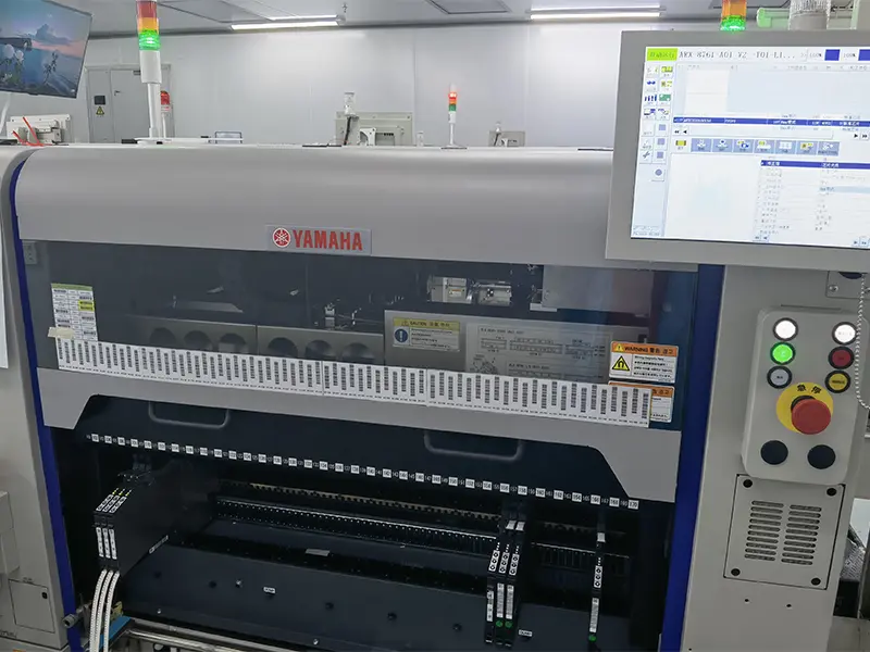
YAMAHA High-Speed Placement
Multi-nozzle YAMAHA mounters delivering ±0.025mm placement accuracy. Effortlessly places 01005 passives, QFNs, CSPs, and fine-pitch BGAs with automated optical fiducial alignment and dynamic feeder calibration.
STAGE 03
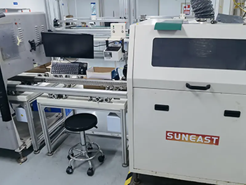
3D SPI & Pre-Reflow AOI
100% inline Solder Paste Inspection evaluates 3D paste height, volume, area, and bridging. Pre-reflow optical inspection halts boards instantly if component displacement, tombstoning, or polarity inversion is identified.
STAGE 04
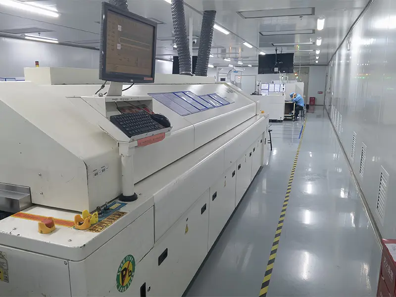
Multi-Zone Lead-Free Reflow
Controlled thermal profiling across 10 upper and 10 lower heating zones. Precise nitrogen (N2) atmosphere prevents intermetallic oxidation on SAC305/lead-free joints, minimizing micro-voiding beneath large thermal pads.
STAGE 05
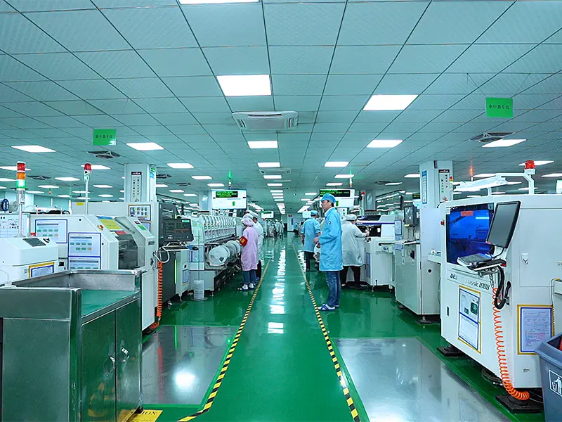
Post-Reflow 3D AOI & AXI
Multi-angle 3D color camera systems calculate solder meniscus angles and fillet heights. Automated X-ray Inspection (AXI) audits hidden BGA ball coplanarity, solder bridging, and void percentages to guarantee IPC Class 3 compliance.
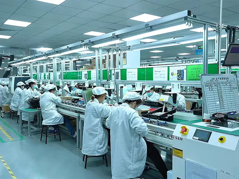
STAGE 06
Parallel SMT Line Architecture
6 independent production lines allow dynamic allocation. Rapid NPI prototypes (1–500 pcs) run on fast-changeover lines without holding up ongoing volume batches, achieving a 97%+ on-time shipping delivery record.
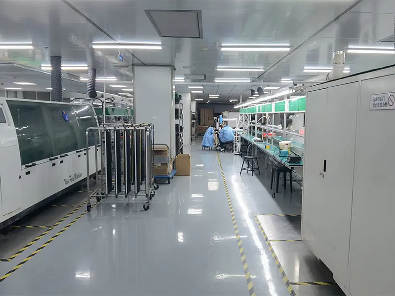
STAGE 07
DIP & Selective Wave Soldering
4 specialized through-hole lines equipped with nitrogen wave soldering and automated selective soldering nozzles. Ideal for high-current relays, heavy inductors, automotive headers, and terminal blocks.
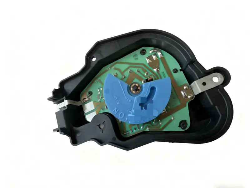
STAGE 08
Box Build, FCT & Aging
Turnkey electro-mechanical assembly including custom CNC/molded enclosures, automated wire harness routing, MCU firmware flashing, automated bed-of-nails functional testing (FCT), thermal burn-in aging, and global logistics.
Future-Ready Engineering
Emerging Trends & Technology Roadmap (2025–2030)
The convergence of edge AI computing, high-frequency communications, and high-voltage e-mobility requires advanced automated assembly solutions.
008004 Placement & Micro-Die Embedding
As wearable medical diagnostics, AR optics, and hearing prosthetics compress silicon real estate, passive component packaging is advancing past 01005 to 008004 (0.25mm × 0.125mm). PCB ADEPT has upgraded solder stencil electroforming and high-magnification optical recognition to place micro-passives with zero solder bridging and negligible component skew.
Wide-Bandgap Semiconductors (GaN & SiC)
Next-generation automotive power trains and industrial converters demand Gallium Nitride (GaN) and Silicon Carbide (SiC) switching speeds. These devices present extreme switching transients and localized thermal densities. Automated manufacturing requires heavy-copper (3oz to 10oz) laminates, direct-thermal-via arrays, and void-free vacuum reflow soldering (<5% voiding).
High-Frequency mmWave & Hybrid RF Stacks
Automated assembly of 24GHz–77GHz radar sensors and satellite phased arrays mandates hybrid multi-layer bonding. SMT machines must handle ultra-low-loss Rogers, Taconic, and Nelco substrates mated with standard FR-4 prepregs. Microstrip trace widths, controlled dielectric constants (Dk), and hard gold finishes ensure minimal insertion loss and tight phase control.
Real-World Applications
Mission-Critical Industry Application Scenarios
Engineered for harsh operating environments, high-reliability lifecycle expectations, and stringent international compliance frameworks.
Automotive & E-Mobility
Use Cases: Battery Management Systems (BMS), On-Board Chargers (OBC), DC-DC converters, and LiDAR driver boards.
- High TG materials (TG170–TG300) resisting extreme under-the-hood heat.
- Conformal coating (acrylic, polyurethane, or silicone) protecting against road grime and salt mist.
- IPC Class 3 solder joints resistant to sustained engine vibration.
Aerospace & Anti-Drone
Use Cases: C-UAS drone jammers, RF power amplification, phased array receivers, and satellite telemetry modules.
- High-frequency Rogers PTFE laminates with immersion gold (ENIG / ENEPIG) plating.
- Precision RF shielding cans placed automatically over synthesizer blocks.
- Full traceability lot tracking for military-grade compliance and reliability.
Medical Diagnostics & Health
Use Cases: Patient vitals monitors, portable ultrasound transducers, lab spectrometers, and wearable ECG monitors.
- Rigid-flex 4–16 layer topologies fitting tight organic ergonomic enclosures.
- Lead-free (RoHS) bio-compatible assembly and zero flux residue cleaning.
- 100% functional testing (FCT) logging full waveform validation before shipment.
Edge Computing & Smart IoT
Use Cases: Raspberry Pi HAT expansion cards, industrial gateway computers, LoRaWAN smart grid meters.
- Multi-layer HDI designs with micro-vias down to 0.1mm laser-drilled.
- Turnkey box-build integration: injection molding, laser engraving, and retail packaging.
- Competitive BOM cost optimization via direct component factory inventory.
Engineering Problem Solving
Overcoming Common PCB Assembly Failure Modes
How PCB ADEPT's advanced automated production safeguards overseas buyers against expensive field failures.
Eliminating BGA Solder Voiding & Bridging
The Bottleneck: High thermal mass chips (FPGAs, GPUs, SoC processors) frequently trap flux volatiles during reflow, creating large voids (>25%) or bridging adjacent solder balls on fine-pitch 0.4mm matrices.
Our Automated Solution: We deploy nanotech-coated electroformed stencils with micro-apertures tailored to solder volume ratios. Multi-zone reflow ovens incorporate dynamic nitrogen purges, maintaining peak temperature delta-T within ±1.5°C across the board. Every BGA joint undergoes Automated X-Ray Inspection (AXI) to guarantee voids remain below 10%, well beyond IPC Class 3 minimums.
Mitigating Rigid-Flex Delamination & Tear
The Bottleneck: Combining flexible polyimide cores with rigid FR-4 prepregs often introduces coefficient of thermal expansion (CTE) mismatches, resulting in pad delamination at transition interfaces during lead-free soldering cycles.
Our Automated Solution: We implement custom-milled aluminum pallet carriers that restrain flexible segments while exposing SMT pads. Polyimide layers undergo pre-assembly vacuum baking at 120°C for 4 hours to eliminate hygroscopic moisture before reflow, preventing outgassing and micro-fractures in flexible vias.
Supply Chain Obsolecence & Counterfeit Shielding
The Bottleneck: Counterfeit active components, grey-market remarking, and sudden IC end-of-life (EOL) announcements cause severe production delays and erratic field burnouts for hardware startups.
Our Automated Solution: Our 10+ year veteran component procurement division enforces strict chain-of-custody sourcing directly with authorized franchises (TI, ADI, ST, Microchip, Murata, TE Connectivity). In-house engineering suggests verified drop-in second-source alternatives during initial DFM, insulating your build against global supply shocks.
| Capability Parameter | Prototype Quick-Turn (NPI) | High-Volume Automated Production | Quality Verification Standard |
|---|---|---|---|
| Layer Count Range | 1 – 32 Layers (Rigid / Flex) | Up to 60 Layers (HDI / Hybrid) | IPC-6012 Class 3, UL 94V-0 |
| Smallest SMT Package | 01005 (0.4mm × 0.2mm) | 01005 to 008004 supported | High-resolution optical alignment |
| Fine Pitch BGA / QFP | 0.35mm ball pitch, 0.3mm lead pitch | 0.30mm ball pitch with underfill | 100% 3D AOI & Automated X-Ray |
| Lead Times | 3 – 9 Business Days | 15 – 25 Business Days | MES-managed live scheduling |
| Solder Paste Chemistry | SAC305 Lead-Free (RoHS compliant) | Low-temperature & High-reliability alloys | Inline 3D SPI (Volume/Height) |
| Supported Substrates | FR-4 (Tg150–Tg180), Polyimide | Rogers, Taconic, Heavy Copper (1–10oz), Aluminum | Thermal stress & IPC microsectioning |
| Batch Order Volume | 1 – 500 Pieces (Fast NPI) | 1,000 to 500,000+ Units | First Article Inspection (FAI) log |
Advanced Substrates & Build Options
Specialized PCB Technologies & High-Frequency Substrates
From 60-layer backplanes to microwave radar laminate boards, our automated factory delivers factory-direct consistency and comprehensive signal loss management.

Buy High Density Interconnect PCB Suppliers in China - Quality HDI PCB from Reliable Factory Pricelist, Factories
Configure Specs & RFQ
ODM China Raspberry Pi HAT Suppliers: Affordable Factory Solutions for Learning and IoT Projects Companies, Pricelist
Configure Specs & RFQ
Famous High-Quality Rigid Flex PCB Manufacturers in China - 1 to 16 Layers Flexible Circuit Boards Supplier Factory Pricelist, Factory
Configure Specs & RFQ
Famous High TG PCB Manufacturers, Company
Configure Specs & RFQ
Famous High-Quality 1-60 Layers Multilayer PCB Factory in China - Fastest Lead Time 48 Hours - Trusted Suppliers Suppliers, Pricelist
Configure Specs & RFQ
ODM High Frequency PCB Solutions from China Suppliers | Factory-Direct Signal Loss & EMI Management Supplier, Quotes
Configure Specs & RFQ
ODM High-Frequency PCB Solutions: China Suppliers & Factory for Signal Loss, Crosstalk, EMI, and Impedance Matching Manufacturer, Supplier
Configure Specs & RFQ
Famous High-Quality RF & Microwave PCBs from China Suppliers - Precision Impedance Control for ≥500MHz Frequency Applications Manufacturers, Supplier
Configure Specs & RFQ
Procurement & Engineering Guide
Frequently Asked Questions on Automated PCB Assembly
Authoritative technical guidance for hardware designers, VP of Engineering, and international procurement managers vetting Chinese EMS partners.
What specific engineering files are required to quote and begin automated SMT assembly?
To generate a complete Design for Manufacturability (DFM) review and an exact quote within 24 hours, send us:
- Gerber or ODB++ files: Providing all copper layers, solder mask, silkscreen, drill files, and mechanical outline.
- Complete Bill of Materials (BOM): Formatted in Excel or CSV with exact Manufacturer Part Numbers (MPN), approved second-source alternatives, reference designators, package footprints, and part descriptions.
- Centroid / Pick-and-Place File: Supplying X-Y coordinates, board surface (Top/Bottom), and rotation angles for automated placement feeders.
- Assembly Drawings & Special Instructions: Indicating testing procedures, conformal coating boundaries, or required firmware flashing scripts.
How does automated 3D SPI and AOI inspection prevent field failures compared to visual checks?
Manual visual inspection with stereo microscopes is prone to eye fatigue and cannot detect volumetric or hidden solder flaws. Our inline 3D Solder Paste Inspection (SPI) evaluates every printed pad using phase-shift moiré interferometry, verifying solder paste height and volume before component placement.
Post-reflow 3D Automated Optical Inspection (AOI) utilizes multi-frequency structured light to measure the solder meniscus curvature, accurately detecting micro-tombstoning, component polarity reversal, and coplanarity issues. For hidden arrays (BGAs, CSPs, QFN thermal pads), Automated X-Ray Inspection (AXI) measures solder void area percentages to guarantee joints withstand prolonged thermal cycling in mission-critical environments.
Post-reflow 3D Automated Optical Inspection (AOI) utilizes multi-frequency structured light to measure the solder meniscus curvature, accurately detecting micro-tombstoning, component polarity reversal, and coplanarity issues. For hidden arrays (BGAs, CSPs, QFN thermal pads), Automated X-Ray Inspection (AXI) measures solder void area percentages to guarantee joints withstand prolonged thermal cycling in mission-critical environments.
Can PCB ADEPT source hard-to-find active semiconductors and verify their authenticity?
Yes. Our veteran procurement team maintains direct relationships with authorized global semiconductor franchises (including Texas Instruments, Analog Devices, STMicroelectronics, Microchip, Murata, and TE Connectivity). We also keep a substantial internal safety stock of high-demand passive passives, microcontrollers, and interface ICs.
Every incoming shipment undergoes rigid Incoming Quality Control (IQC) inside our ESD-controlled warehouse: decapsulation analysis when required, package verification against manufacturer datasheets, moisture sensitivity verification (baking in dry cabinets), and solderability testing before components enter the automated SMT staging feeders.
Every incoming shipment undergoes rigid Incoming Quality Control (IQC) inside our ESD-controlled warehouse: decapsulation analysis when required, package verification against manufacturer datasheets, moisture sensitivity verification (baking in dry cabinets), and solderability testing before components enter the automated SMT staging feeders.
What are your prototype NPI vs. mass production delivery timelines?
For New Product Introduction (NPI) prototypes ranging from 1 to 500 pieces, typical turnaround is 3 to 9 business days from BOM component kitting completion. Urgent bare board quick-turns can be fabricated in as little as 24 to 48 hours for multilayer prototypes.
For mid-to-high volume scheduled production runs (1,000 to 500,000+ units), standard lead times run between 15 to 25 business days, supported by dedicated automated SMT lines and kanban safety stock agreements to insulate overseas clients against sudden market spikes.
For mid-to-high volume scheduled production runs (1,000 to 500,000+ units), standard lead times run between 15 to 25 business days, supported by dedicated automated SMT lines and kanban safety stock agreements to insulate overseas clients against sudden market spikes.
Do you offer turnkey electro-mechanical box-build assembly and firmware programming?
Yes, PCB ADEPT operates as a full-service Electronic Manufacturing Services (EMS) provider. Beyond surface mount PCBA, our engineering team manages:
- Plastic injection tooling, enclosure molding, silicone keypad casting, and precision aluminum CNC machining.
- Automated firmware flashing via dedicated gang programmers or JTAG test headers.
- Custom bed-of-nails Functional Circuit Testing (FCT) jigs executing live power-up, RF frequency calibration, and sensor simulation.
- Environmental aging (thermal cycling and burn-in chambers).
- Retail box packaging, custom barcode labeling, and direct global drop-shipping via DHL, FedEx, UPS, or air/ocean freight.
Accelerate Your Hardware with an Automated Assembly Leader
Send your Gerber files, BOM, and assembly specifications directly to PCB ADEPT's engineering desk in Bao'an, Shenzhen. Receive comprehensive DFM analysis, component availability screening, and an itemized quotation within 24 hours.