
High-Quality Multilayer PCB Manufacturer, Companies
Product Description
1. Definition of a Multilayer PCB
The core advantage of multilayer PCBs lies in their ability to implement complex wiring within limited space, meeting the miniaturization and high-performance requirements of electronic products. They are widely used in smartphones, servers, medical devices, and other fields.
Made of copper foil to transmit electrical signals and distributed power.
Primarily composed of prepregs (e.g., epoxy resin) ensuring insulation between copper traces.
Shields and protects delicate circuits against unintended bridges and short circuits.
Prevents bare copper oxidation and ensures dependable component solderability.
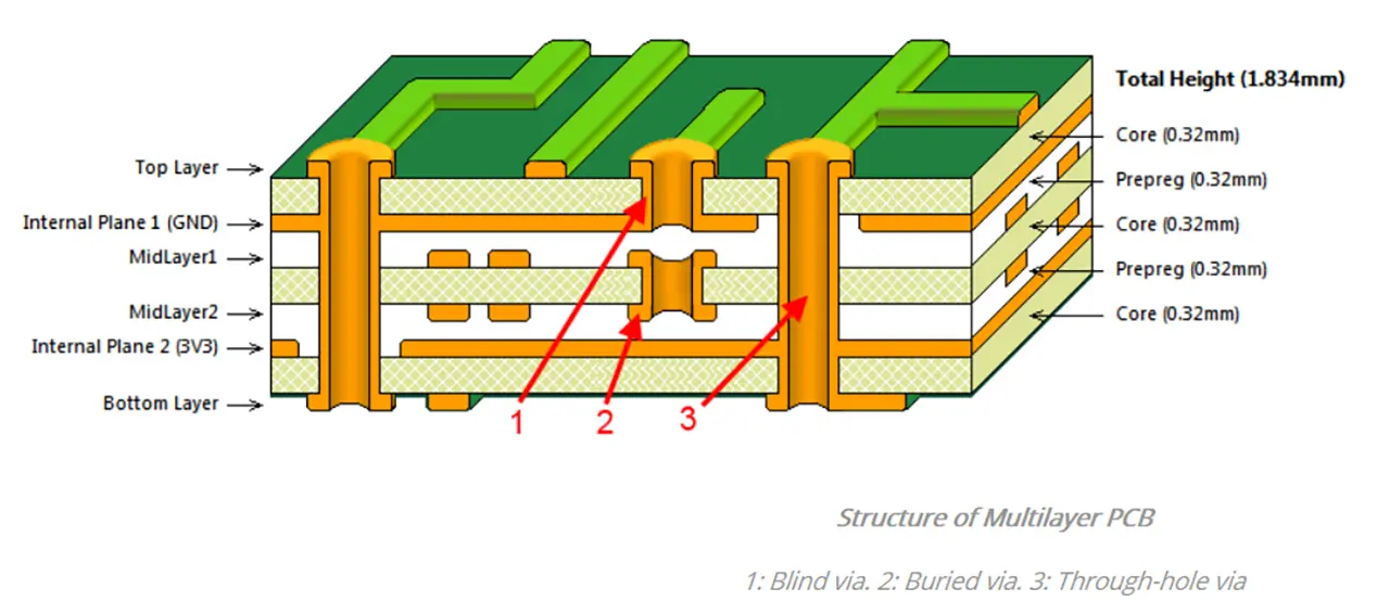
The diagram below shows the stackup structure of a 6-layer 1-step HDI (High-Density Interconnect) multilayer PCB, illustrating its layer stacking and via design:
2. Core Design Challenges and Solutions
| Design Challenge | Specific Issues | Solutions |
|---|---|---|
| Signal Integrity | High-speed signal transmission is prone to reflection and crosstalk, leading to signal distortion. The risk of crosstalk increases with more layers. |
• Adopt equal-length differential routing; maintain spacing of ≥ 3x line width for high-speed signals. • Add matching resistors (e.g., 50Ω) at the signal source. • Route high-speed signals in inner layers and isolate interference with solid ground planes. |
| Power Integrity | Power planes suffer from noise and voltage fluctuations; multiple voltage supplies are prone to mutual interference, causing chip crashes. |
• Arrange power layers adjacent to ground layers for filter capacitor coupling. • Place decoupling capacitors (e.g., 0.1μF) directly near chip pins. • Split power planes carefully and isolate cross-split areas with ferrite beads. |
| Wiring and Routability | Increased layer counts result in limited routing space; dense areas become disorganized and difficult to route. |
• Layout by functional partitions and group associated components together. • Route high-speed signals through inner layers and keep low-speed control traces on outer layers. • Appropriately reduce the width of non-critical signal traces to preserve routing channels. |
| Heat Dissipation | High-density component placement causes localized heat accumulation around high-power ICs, degrading reliability. |
• Drill 1–3mm thermal vias directly beneath heat-generating components. • Pour large-area thermal copper planes or mount dedicated heat sinks. • Disperse high-power devices and align layouts with chassis cooling airflow paths. |
| Interlayer Alignment & Process | Higher layer counts require repeated lamination cycles; copper foil shift (>30μm can trigger shorts) and drilling fractures are typical. |
• Select advanced materials like ultra-low profile copper foil. • Deploy high-precision laser drilling systems to hold tolerances within ±15μm. • Utilize vacuum laminators to minimize pressure fluctuations during heating cycles. |
3. Key Considerations for Multilayer PCB Fabrication
Multilayer PCB fabrication involves high process precision. Parameter variations or improper execution at any stage—from base material selection to shaping and testing—can compromise the entire assembly. Critical parameters include:
- Material Matching: Specify substrates matched to performance targets. Standard FR-4 fits mainstream consumer electronics, whereas Rogers (low dielectric loss) or polyimide (high temperature limits) are essential for high-frequency RF and aerospace designs.
- Copper Foil Dimensioning: Select foil weights based on current carrying requirements to restrict thermal buildup. Control prepreg resin ratios tightly to prevent delamination and preserve signal integrity.
- Circuit Patterning & Surface Preparation: Transfer circuits via precise exposure and development, carefully controlling etch parameters to eliminate residual copper or line narrowing. Apply black or brown oxidation to roughen copper boundaries and optimize lamination adhesion.
- Stackup Alignment: Align inner cores, prepregs, and external foils in strict conformance with the design stack to prevent layer misregistration.
- Thermal & Pressure Control: Regulate temperatures strictly at 180–220℃ with pressures maintained at 3–5MPa under tightly controlled dwell cycles to eradicate air bubbles and resin starvation.
- Symmetrical Architecture: Enforce even-layer counts with balanced stackups around the central core to eliminate warpage and bow/twist after cooling.
- High-Precision Drilling: CNC drilling machines must keep standard through-hole diameters above 0.2mm with positional accuracy within ±0.05mm. Appropriately specify through-holes, blind vias, and buried vias to avoid needless build costs.
- Hole Wall Metallization: Deposit uniform copper via sequential electroless and electrolytic plating. Thorough desmear and chemical cleaning are mandatory to prevent plating voids, blistering, or inner-trace separation.
- Outer Circuit Processing: Execute fine-pitch photolithography and etching without burrs or hairline bridging, ensuring optimal solderability.
- Surface Finish Options:
• HASL (Hot Air Solder Leveling): Robust and cost-effective, suited for general consumer products.
• Immersion Gold (ENIG): Outstanding planar surface, perfect for high-density BGA packages and high-reliability gear.
• OSP (Organic Solderability Preservative): Economical and planar, though sensitive to prolonged storage and high thermal exposure.
- Profile Machining: CNC route board outlines holding tolerances within ±0.2mm. Retain 3–5mm processing breakaway rails to streamline SMT placement.
- Quality Verification: Utilize AOI (Automated Optical Inspection) for visual defects, Flying Probe / ICT fixtures for impedance validation (within ±10%), and industrial X-ray systems to evaluate internal blind/buried via registrations.









