Pcba Manufacturing turns an electrical design into a working, testable circuit board. It combines printed circuit boards, electronic components, solder, software, and disciplined inspection. The process may look mechanical, but every placement matters. A misplaced resistor can stop an entire product.
Market demand continues to grow. The World Semiconductor Trade Statistics Spring 2024 Forecast valued global semiconductor sales at approximately 611.2 billion US dollars for 2024. It projected about 687.4 billion US dollars for 2025. These figures do not measure PCBA production directly, but they show the expanding component base behind automotive, medical, industrial, and consumer electronics. IPC’s Electronics Industry Impact Study also places the global electronics ecosystem at roughly 5 trillion US dollars annually. That scale creates opportunity, but it raises quality expectations.
A typical assembly begins with solder-paste printing on copper pads. Pick-and-place machines then position components with precise coordinates. Reflow ovens heat the board through controlled temperature zones. Operators and automated optical inspection systems check solder joints, polarity, and missing parts. Functional testing follows.
Small details matter.
Reliable manufacturers often follow IPC-A-610 and J-STD-001 requirements. They may also use ISO 9001 quality systems, traceability records, and process capability data. However, no production line is flawless. Moisture, warped boards, poor footprints, and incomplete design files can still create defects. I have found that the most useful manufacturing decisions happen before assembly begins. Clear documentation, realistic tolerances, and early design-for-manufacturing reviews can prevent expensive rework later.
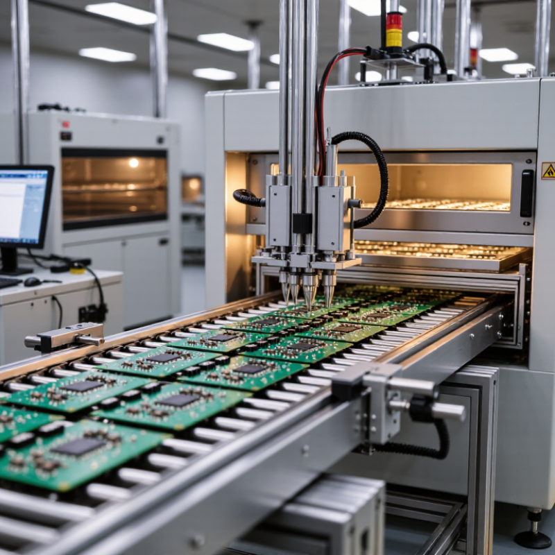
PCBA manufacturing means assembling electronic components onto a printed circuit board. In IPC terminology, a PCB is the bare board. A PCBA is the populated and soldered assembly. This distinction matters during purchasing, inspection, and production planning.
The process usually begins with a design review and component verification. Machines place tiny surface-mount parts onto solder paste. Larger parts may use through-hole technology and pass through a separate soldering step. Technicians then inspect solder joints with optical systems or X-ray equipment when hidden connections require checking. Functional testing can confirm whether the finished assembly performs as designed. IPC terminology helps teams describe defects, workmanship, and acceptance requirements consistently. Still, terminology alone cannot fix a weak design.
Tips: Ask for the required IPC class before production begins. Confirm component orientation, polarity, and approved substitutions. Keep clear records of inspection results and rework. A small labeling mistake can delay an entire batch.
In real production, problems often appear at the boundaries between design and assembly. A pad may be too small for reliable soldering. A connector may fit the drawing but fail during repeated use. Experienced teams review these risks before releasing files. They also examine moisture-sensitive components, thermal limits, and board cleanliness. These checks are practical, not decorative. Even careful processes need improvement, because first-pass success is never guaranteed.
PCBA manufacturing begins long before components reach an assembly line. Design teams first choose materials that match temperature, frequency, strength, and cost requirements. Common choices include glass-reinforced laminate, copper foil, solder mask, and protective surface finishes. IPC-2221 provides useful guidance for insulation spacing, conductor sizing, and mechanical design. However, it is a design framework, not a substitute for engineering judgment.
Real products demand careful DFM reviews.
Engineers check trace widths, via sizes, annular rings, board thickness, and component clearances. They also inspect thermal paths around power components. A small clearance error can create solder bridges or prevent reliable inspection.
It looks minor. It is not.
Once fabricated, the bare PCB receives solder paste through a controlled stencil process. Automated placement positions components against the assembly drawing. Reflow heat then melts the paste and forms electrical joints. Through-hole parts may require a separate soldering step. Optical inspection, electrical testing, and careful sampling reveal weak joints or misplaced parts. In practical projects, the first design pass is rarely perfect. I have seen a connector fit mechanically but block a test probe. That mistake changed the layout more than the circuit itself. DFM works best when manufacturing, assembly, and testing teams review the design together. Still, IPC-2221 cannot predict every factory variation, so measured results should challenge the original assumptions.
PCBA manufacturing turns a bare circuit board into a tested electronic assembly. Stencil printing starts the process. A metal stencil aligns over the board, while a squeegee pushes solder paste through tiny apertures onto copper pads. The paste volume matters. Too much can create bridges; too little can produce weak joints. IPC-7525C identifies stencil design, aperture geometry, and paste control as key process considerations.
SMT placement follows. Automated placement equipment picks components from feeders and places them onto the printed paste. Modern systems can advertise speeds approaching 100,000 components per hour, but that figure is usually theoretical. Real throughput drops when boards contain fine-pitch packages, large connectors, rotating parts, or frequent feeder changes.
A practical line may spend more time correcting placement errors than expected. That detail is often overlooked.
Industry data shows why speed remains important. The World Semiconductor Trade Statistics forecast semiconductor sales at 611.2 billion US dollars for 2024, increasing pressure on manufacturers to expand capacity. Meanwhile, IPC research continues to identify supply-chain volatility, labor availability, and quality control as major electronics manufacturing concerns. In production, operators commonly verify paste deposits with solder-paste inspection before placement continues. Placement data, feeder status, and inspection results should also be tracked together. A fast machine is not automatically an efficient line. Scrap tells the truth.
What Is PCBA Manufacturing and How Does It Work?
Lead-Free Reflow Soldering: SAC Alloys Melt at Approximately 217°C
PCBA manufacturing converts bare circuit boards into working electronic assemblies. Screen printing deposits solder paste onto copper pads. Pick-and-place equipment positions components with high accuracy. The populated board then enters a controlled reflow oven.
SAC alloys melt at approximately 217°C. The exact liquidus range depends on alloy composition, as reported in IPC J-STD-006. A typical lead-free profile reaches about 235–250°C, while the board remains above liquidus for roughly 45–90 seconds. IPC-7530 recommends controlling ramp rates, soak conditions, peak temperature, and cooling speed. These values protect small components from thermal shock.
Temperature matters more than speed.
Technicians place thermocouples near large ground planes, fine-pitch packages, and board edges. A single oven setting cannot heat every location equally. The center may reach the target temperature, while a heavy copper area remains below 217°C. That condition can create dull joints, voids, or incomplete wetting. A higher peak may correct one area but damage another.
NIST thermophysical data supports careful interpretation of alloy melting behavior, rather than relying on nominal labels alone. X-ray inspection helps measure hidden voids beneath area-array packages. Automated optical inspection checks visible solder shapes, but it cannot confirm every internal defect. In practice, a “good” first pass may still need profile adjustment. Manufacturing data deserves more trust than appearance.
In PCBA manufacturing, IPC-A-610 defines visual acceptance criteria for assembled boards. Class 1 covers general products with limited operating demands. Class 2 applies to equipment needing reliable, continuous service. Class 3 targets high-performance systems, where downtime or failure may create serious consequences. The class must match the product’s real environment, not simply the customer’s preference.
Inspectors examine solder joints, lead protrusion, component placement, board damage, and contamination. Automated optical inspection can detect shifted parts and visible solder defects. X-ray inspection reveals hidden voids or incomplete joints under packages.
Electrical testing adds another layer. In-circuit testing checks nets and components, while functional testing confirms actual operation. IPC-A-610 is an acceptance standard, not a substitute for a complete test strategy.
Quality teams should record first-pass yield, defect-per-million opportunities, repair rates, and false calls. NIST Manufacturing Extension Partnership guidance commonly places poor-quality costs near 15–20% of sales, with higher exposure in unstable processes. IPC’s 2024 Global Sentiment of the Electronics Industry report also highlights continuing material, labor, and delivery pressures. These conditions make traceable inspection data valuable. Still, a perfect AOI image proves little if the test fixture is poorly designed. Class 3 does not remove engineering judgment. Sometimes, the hardest decision is admitting that the chosen class was wrong.
It means mounting and soldering electronic components onto a bare printed circuit board. The finished board becomes a populated assembly.
A PCB is the bare board. A PCBA includes placed components, solder joints, and completed assembly work.
The process includes design review, component verification, solder paste printing, component placement, reflow soldering, inspection, and testing.
Surface-mount parts sit on solder paste and pass through reflow heating. Larger through-hole parts may need separate soldering.
DFM reviews check trace widths, via sizes, clearances, board thickness, and thermal paths. Small errors can cause solder bridges or blocked test access.
Common materials include glass-reinforced laminate, copper foil, solder mask, and protective surface finishes. Selection depends on heat, frequency, strength, and cost.
Optical inspection can find visible defects. X-ray inspection may reveal hidden connections, while electrical testing checks circuit performance.
Confirm the required quality class, component orientation, polarity, approved substitutions, and inspection records. Labeling deserves attention.
No. A first-pass failure can still happen because design assumptions meet real factory variation. Measured results should challenge the original plan.
A pad may be too small, or a connector may block a test probe. These details seem minor. They can force layout changes.
Pcba Manufacturing is the process of transforming a bare printed circuit board into a complete, functional assembly by attaching and soldering electronic components. The work begins with material selection and design-for-manufacturing planning in accordance with IPC-2221 principles, helping ensure that board layouts, spacing, and component choices support reliable production. Once the bare PCB is prepared, solder paste is applied through a stencil, and automated surface-mount technology places components at high speed, with advanced lines capable of positioning up to 100,000 components per hour.
After placement, the assembly passes through lead-free reflow soldering, where SAC alloys melt at approximately 217°C to create secure electrical and mechanical connections. Final inspection and testing verify workmanship, component placement, solder quality, and functional performance. IPC-A-610 acceptance Classes 1, 2, and 3 provide different criteria based on the product’s reliability and operating requirements, ensuring that each PCBA meets its intended quality standard.